This thread has been locked.

If you have a related question, please click the "Ask a related question" button in the top right corner. The newly created question will be automatically linked to this question.

LM51521-Q1: getting Pspice for TI error when I try to "Open Model Test Circuit"

Part Number: LM51521-Q1
Other Parts Discussed in Thread: PMP30963, CSD18536KTT, CSD17318Q2, LM5152-Q1, LM5152EVM-BST, CSD17581Q3A, LM5176

Hello Team,

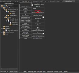
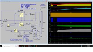
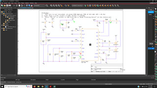
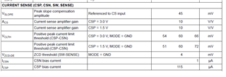
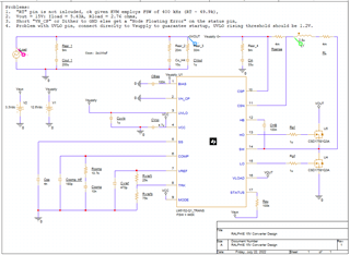
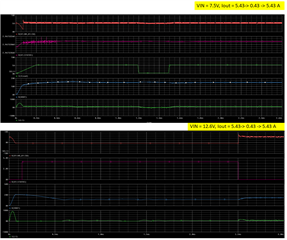
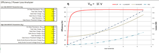
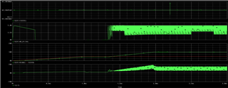
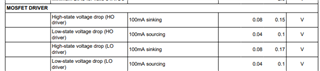
My customer gets the following error (see attached pic) when they try to open the parts reference transient simulation/design.

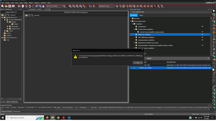
 Any thoughts on how to get past this problem?

Regards,

Renan

  • Hello Renan,

    Thanks for reaching out to us.

    We will look into it and come back to you by tomorrow.

    Best regards,

    Harry

  • Hi Renan,

    I just checked our PSpice library and unfortunately, there is no PSpice reference model supporting the LM5152 yet.
    Instead, I would recommend using the the normal PSpice transient model (just the IC) from the PSpice for TI library, or per download from the product page, and take the Quickstart calculator or reference design (PMP30963) for guidance.
    https://www.ti.com/product/LM5152-Q1#design-tools-simulation
    https://www.ti.com/tool/PMP30963

    Please let me know if you have additional questions.

    Best regards,
    Niklas

  • Hello Niklas,

    Good day and thank you for this response. Please see my customer response below:

    I am using PSPice for TI to recreate the part's EVM model/schematic as close as I can.
    I am getting the following odd "floating node" error (see attached pic) on the "status" pin.
    Not sure why I am getting this error. Same error if I tie it to a 3.3V, ground or unconnected.Attached the complete project (see attached zip file).
    Would someone please help me get past this error?

    Help.zip
    Regards,
    Renan

  • Hi Renan,

    Thanks for the feedback.
    I will have a look at the model and will get back to you by the end of the week.

    Best regards,
    Niklas

  • Hello Niklas,

    Good day. While your are working on the first question concerning the "floating pin problem" please see other inquiry provided by my customer below:

    1. How exactly does one determine parts "Rcomp", "Comp" and "Chf"? I employed all of the recommend components from the parts "Quickstart calculator". I also understand these components are compensator components though one must first be able to determine a system's open loop gain (Tu) before one make compensator decisions and close the loop (T) via the compensator. I ask because the open/closed loop gain is not completely obvious i.e. the path from a feedback pin to a control signal. Generally part data sheets have some rough description of this path. Perhaps someone from your group has already written a white paper on this very topic. Please let me know.

    2. Also trying to determine N ch Mosfets for my particular application (see attached quickstart calculator excel sheet for my setup). The parts EVM board employed the following appropriately oversized part:
    NVMFS5C645NLWFAFT1G
    Which are no longer available.
    Looking at TI N ch Mosfets I came across the following:
    The first, csd18536ktt, is a close match to the EVM mosfet.
    The second, csd17318q2, appears to be designed for low VGS parts like this boos controller part.

    Curious as to why the EVM design did not employ a TI Mosfet?

    Does TI have a good white paper/tool to help determine the best Mosfet for my particular application?

    Regards,

    Renan

  • Hi Renan,

    Here is also an update from my side:

    I still haven't found the source for the "floating pin" error. I do not assume, that there is a mistake in the model, as it is functioning just fine for other circuits. It might be some internal paths, which make the model think the status pin is floating in the current state.
    I will dig deeper and see if I can find a solution.

    The customer also commented, that there is no RT pin. Even thought this pin is not existent, the switching frequency can be changed, by setting a different value in the properties.

    Follow-up question 1:
    There is an application report on system stability, which I find very helpful.
    https://www.ti.com/lit/an/slva381b/slva381b.pdf
    It explains the connection of bandwidth and phase margin, and their impact on the stability of a system. These are also the parameters, the quickstart calculator mentions. It is true that not only the compensation has an impact on the stability, but also the feedback resistor, the output capacitance & ESR, the inductor and the MOSFET resistance.
    The calculator takes most of these values into account.

    Follow-up question 2:
    Unfortunately, I do not have much experience on optimizing MOSFET choices. There is not much documentation on FET selection in the datasheet of the LM5152 either. It is highly important that the voltage rating of the FET can withstand the maximum switch node voltage, while additionally leaving some margin for safety. Additionally, a low on-resistance value can have a positive influence on the efficiency and also impacts the stability.

    I will get back to you next week with an update on the floating pin issue.
    If you have any additional questions in the meantime, please let me know.

    Best regards,
    Niklas

  • Hello Niklas,

    Please see my customer response below:

    1. Perhaps it may be faster if a pro your group where to build either a TINA or PSpice for TI simulation employing part LM5152-Q1. You could recreate the circuit employed in the "LM5152EVM-BST User's Guide.pdf" (see attached). Once I have a working simulation then I can make the mods unique to my IO,

    2. How exactly are the compensator components (Rcomp, Ccomp, CHF) determined? It does not appear as though the parts spec nor its quick start calculator excel doc show explain exactly how they are calculated. I am guessing an outer voltage loop encloses an inner current loop (see attached "inner outer loop.png", I just have not seen such a two loop system implemented as displayed on either page 14 or 24 of the part's data sheet.
    I can probably work it out though I'd like to double check my results against a pro from TI who has probably already worked it out.

    Another question,
    I want to make sure that equation 11 (10*Rs*Ipk = 0.6V)
    1. Section 8.5 defines VCLTH as 60 mV (nominal),
    2. Section 9.2 appears to illustrate a "Peak C/L Comparator" with VCS and VCLTH as inputs,
    3. Figure 9-16 illustrates a "Current Limit Comparator" with VCS and 0.6V as inputs,
    4. Finally, finally figure 9-17 compares VCS (10*RS*ILpk) vs 0.6V.

    I may be reading things wrong though it appears as though equation 11 is correct i.e. 10*Rs*Ipk = 0.6 though I think that figures 9-16 and 9-17 are labeled wrong. 0.6V should be replaced with either 0.06V or VCLT.

    8664.Attachment.zip

    Please let me know what is correct.

    Regards,

    Renan

  • Hi Renan,

    Sadly, our library only provides a PSpice model for the LM5152 at the current state.
    However, I think I found the source of the floating pin error. The error message marked the Status pin of the IC, but it seems the issue tracks back to the VH_CP pin (pin 2), which is connected to CDither cap to ground in the customer model.
    For debugging, I recommend to set this pin to GND and disable its function. Afterwards the model should not throw a convergence error anymore.
    Please let me know, if the customer can successfully solve the PSpice issue this way.

    I will also take a look at the compensation calculations from the second question and get back to you before the end of the week.

    Best regards,
    Niklas

  • Hello Nikals,

    Please see the response from my customer:

    Would you please send me the values of the internal feed back resistors (FB voltage voltage divider - see attached).

    Once I have these I should be able to complete the voltage compensator.

    Also, what is the gain bandwidth product of the voltage compensator amp (amp next to the FB pin).

    Attached the current Pspice for TI project using LM5152 - I shorted "VH_CP" or the dither pin to get past the "status pin floating error".
    Also attached the corresponding excel quickstart calculator for IO.

    How does one control the start-up inductor current?

    I started with the recommend Css value then incremented though I saw now change. Rcs was selected such that current limiting should enable around a ILpk of about 6.77A though in the attached figure ILpk gets to about 70 amps.
    Pretty sure that I implemented all components derived in the excel quickstart calculator

    Attachment(2).zip

    Regards,

    Renan

  • 1_LM5152EVM_BST_Users_Guide PSpice for TI.zip

    Niklas,

    I am the progenitor of these LM5152 (boost) questions (started with the node floating error).  Hopefully I can fit my current state and questions in this posting:


    1.  "1_LM5152EVM_BST_Users_Guide PSpice for TI.zip"  contains the current state of my PSpice for TI transient simulation, follows the TI EVM board and uses parts derived from the parts quickstart calculator (attached),

    LM5152-Q1_Excel_Quickstart_Calculator_for_Boost_Controller_Design 8V5.xlsx

    2.  "schematic.png" is a picture of the PSpice for TI schematic,

    3.  "simulation results.png" is the simulation results from 2.  The point of this picture is to 1. demonstrate that the output voltage is lower than expected (designed for 8.5V and seeing something around 8.0V) and 2. the "VREF" pin is at zero volts.  VREF = 1V is required to properly setup TRK and therefore VOUT - something is wrong here and 3.  Startup inductor current experiences large inrush current.  I was hoping that this chip had a solution for the boost inrush current problem.  Perhaps it does not.  Does PSpice for TI have NTC resistors that I can drop in?

    4.  "schematic different probes.png" similar to 2 though probes on the FETS,

    5.  "simulation results different probes.png" is the simulation results from 4.  The point of this picture is to demonstrate there is no switching going on i.e. the top switch is constantly on and the bottom switch is constantly off.  Is this Pspice model a transient or average model????

    6.  "3_Boost_CPM_CL_VA_set.png" was meant to demonstrate that I know how to at least setup an LTSpice simulation of a boost switching converter via CPM and voltage control (inner/outer control loops) and that I know how properly setup its corresponding small-signal model to build appropriately sized compensator components i.e. I kind of know what I am doing.

    7. I understand that this part employs an OTA type II voltage compensator though I do not believe the gain of this OTA is provided (the gain of the current sensed amp is provided, 10 V/V) nor its resistor divider values (see TI "slva662.pdf").  I should be able to design and model closed loop gain of the circuit and derive Rcomp, Ccomp and CHF if given these values.

    Priorities:

    1.  I think there is something wrong with the parts PSpice model - see 1 - 5 above.  I'd really like to see this simulation working properly before I recommend purchasing it.  Please let me know if you agree that something is wrong with the model (I could very well have setup something wrong - I do make mistakes) and if so if/when TI may get this model working,

    2.  I'd like to know the OTA type II resistor divider values and gain - see 7 above,

    3.  I'd also like to know how TI derived Rcomp, Ccomp and CHF.  Someone at TI must have this info somewhere.  I derived these values for my simulation (see 6 above).  I am guessing I that can do the same for this part if I had all the info.

    I apologize for the info dump and questions.

    Thank you,

    Craig

  • Hello Craig and Renan,

    I will let Niklas answer the PSpice questions.
    But with regards to the compensation I will need to make a statement here.

    For the calculation of the external components TI has created the Excel Quickstart Calculator.
    We are glad that we have this tool and our internal engineers rely on it. 
    The equations are protected because some of the parameters that they are using are considered as TI intenal information.

    Please enter the parameters of your power stage into the Quickstart Calculator to calculate the three components of the compensation network, dependent on the components that you chose.
    (TI internally we would do exactly the same.)


    The diagrams which show the internals of our devices are not meant to be accurate schematics which can be used for calculations.
    They are just meant to illustrate the basic principle what is going on inside our part.
    In this case here, it is meant to show that the actual feedback divider is inside the part and how to use the TRK pin instead.
    Again, the exact details are considered as TI intenal information and will not be opened up.
    The parameters that you are asking for are not necessary to operate the part and are therefore not public.
    Even if you had them, I could not guarantee if the diagram of the internal circuitry is complete or if other components around that error amplifier may exist but are not shown there.


    Best regards,
    Harry

  • Hi Craig, Hi Renan,

    I will take a closer look into your design and the LM5152 to find the source of this issue.
    I will get back to middle of next week with more details.

    Regarding point 3.)
    If the PSpice for TI library does not include the needed parts, it is possible to implement third party models. The only downside is, that only three simulation probes can be places simultaneously afterwards.
    A guide on how to include additional model can be found here:
    training.ti.com/pspice-ti-3rd-party-model-import

    Regarding point 5.)
    The description of the model part says if it is the transient or average model.
    LM5152_TRANS means in this case, that it should be the transient model.

    Best regards,
    Niklas

  • Hi Craig,

    I made some simulations with your model and saw the same behavior.
    As the device is not switching, my first assumption was that the device never boots up and stays in shutdown mode.
    When looking at the UVLO/EN pin, I noticed that the lower resistor at the feedback divider (RuvIotb) is only 8Ohms, while the upper resistor is 36kOhms. As a result, the voltage at the UVLO/EN pin is below the threshold of starting up.

    I connected the UVLO pin to Vsupply, to make sure the device starts up in all cases. Afterwards the IC started switching and the output voltage reached the desired 8.5V.

    I would recommend to check the voltage at the UVLO pin from your side as well and see if changes can make the device start up.

    Please let me know, if you can make progress or if further questions arise.

    Best regards,
    Niklas

  • Niklas,

    Good catch!

    I added a "K" to that resistor though I still do not see switching.

    VUVLO (pin) is about 2V and switching does not start.  Increased the bottom resistor to 20k (VUVLO = 2.5V) and it still did not start switching.

    Question 1:

    What exactly is the VUVLO threshold? Is the VUVLO threshold approximately 1.2 V?  I am looking at the rising threshold voltage here.  This value is not obvious to me.


    Connecting the VUVLO pin to Vsupply got the circuit switching.

    Question 2:

    Is there a good reason not to connect Vsupply directly to the UVLO/EN pin?  Based on the data sheet schematic, it does not appear as though this pin is capable of sinking a lot of current.  Just following the data sheet and quickstart calculator.

    I am working on a Question 3 (deals with compensator components),

    Thank you,

    Craig

  • Niklas,

    Question #3 (follow-on from my last set of questions).

    Harry shot down the idea of providing users complete details of the parts inner current and outer voltage loop.

    Pro:  The quickstart calculator does allow one to design/verify a single operating point (Vsupply = fixed1, Iout = fixed1),

    Con:  The quickstart calculator does not allow one verify that a particular compensator design works at the full range of operating points (Vsupply = Vmin/Vmax, Iout = Imin/Imax).

    See attached picture:

    The upper left figure is a Bode plot of the vcontrol to vout (Gvc(s) for a CPM simple approximation model) given the full range of operating points (Vmin/Vmax, Imin/Imax),

    The upper right figure is a Bode plot of the loop gain after closing Gvc(s) with a type II voltage loop compensator given the full range of operating points against the frequency response of the voltage loop compensator transfer function (dark red),

    The bottom figures plots the  corresponding closed loop frequency and step response, again given the full range of operating points.

    Now that I have the part PSpice model working I can verify that the system is stable at the full range of operating points but simulations take a long time, but if any of the operating points are unstable I need to plug and play (given updates to the quickstart guide) until all operating points are met which significantly increases the amount of time that I have to dedicate to this part.

    Please reconsider providing users complete access to the parts inner and outer loops.

    Thank you,

    Craig

  • Niklas,

    Forgot Question #4:

    Do you/TI have a solution for this parts large start-up inrush current?

    I am currently using an ideal source i.e. no series resistance - this would lower inrush,

    I know that the inrush is a function of the size of the output capacitor,

    Problem:  I have looked into sizing an NTC resistor though so far I have not found any that can handle the large continuous input current given my setup (11A continuous).

    Thank you,

    Craig

  • Hello Craig,

    Just to make sure that we are talking about the same thing:

    The inrush current that you mention is the current that charges the output cap (through the body diode of the high-side FET),

    BEFORE the LM51521 even starts operating,

    is that correct?

    Thanks,

    Harry

  • Hi Craig,

    I am glad to hear your model is running now.
    You are correct, that the threshold for the UVLO should be around 1.2V. So it confuses me as well, that the voltage of the UVLO pin needs to be higher in this PSpice model.
    Regarding your second question, I can agree that there should be no disadvantage when connecting UVLO directly to Vsupply. A voltage divider is merely a feature, if undervoltage triggering at a customized voltage is desired.

    Q3) I am sorry that the quickstart tool, showing only one operation situation at the same time, comes at an inconvenience. We constantly try to improve our design tools and resources for our product support, so this feedback is very much appreciated. 
    Giving complete access to detailed design structures is difficult, as this data often includes confidential data, so I hope for your understanding that we cannot provide the full design details for all the TI parts.

    Q4) When looking into the schematic, I would assume that not all the inrush current runs through the FET. A lot of current is needed for the initial charging of input and output caps.
    I recommend to try a simulation with the caps initial conditions (IC) set the their desired operating voltage and check the current flows for both the inductor, diode and mosfet, as well as the softstart behavior.

    Best regards,
    Niklas

  • Niklas,

    How exactly does one determine the working/manufacturing range of VCLTH given CSP (3.0V vs 1.5V given Mode = GND)?

    Mode = GND only applies to a "fixed" skip mode.  I plan to use the FPWM i.e. Mode tied to VCC,

    I do not know how to determine the CSP 3.0 vs 1.5V portion.  So far my worst case peak inductor current is about 12.7 A with an RS of 4mohms so VCSP = 0.0508V.

    Not sure if I should assume VCLTH ranges from 54 to 66 mV or 51 to 72 mV.

    Please let me know which range I should use given my setup.

    Thank you,

    Craig


  • Hi Craig,

    As this question is more about the device and less about modeling, I would pass this one on to Harry, as he knows more about the part itself.
    He is currently out of office until the end of the week, but he returns on monday.

    I will send him a notification and get some feedback from him, so you get a detailed response earlier next week.

    Thanks you very much for your patience.
    Best regards,
    Niklas

  • Niklas,

    What is the best setup to avoid convergence errors for this part?

    I am using parts from the quickstart guide.

    I am leaving the simulation tolerance values at standard.  Generally if I get a convergence error and relax a tolerance the results turn to garbage.

    I get convergence errors with or without capacitor Resr's present.

    I get convergence errors with our without stepping the output.

    I get convergence errors if I change the input voltage from min to max (based on quickstart guide).

    I really cannot tell if I have a part problem, a quickstart compensator problem or a PSpice for TI problem.

    I have been spinning my wheels for days trying to get a decent simulation result.

    Thank you,

    Craig

  • Niklas,

    I attached an example where it took the controller about 2.5 ms to turn on or at least start switching.

    Any thoughts what may be going on here?

    Thank you,

    Craig

      7840.LM5152-Q1_Excel_Quickstart_Calculator_for_Boost_Controller_Design 15V 440 kHz.xlsx

  • Niklas,

    Follow-up simulations results.

    Top pic, Vin = 7.5V, appears to be working.

    Bottom pic, Vin = 12.6V, very long turn-on (switching) delay.

    Furthermore, page 6 of the part's data sheet lists a max HB to SW of 5.8V.  Note 3 of that page threatens de-rated life expectancy when operated over 5V.

    The top plot in each pic plots HB to SW.  Both traces appear to be greater than, if not equal to, 5.8V.

    Is the HB to SW limit written correctly or is the simulation wrong or something else?

    Thank you,

    Craig

  • Niklas,

    Also appears as though the status pin is not working quite right.

  • Hi Craig,

    Thanks for sending more details.
    Regarding PSpice convergence issues:
    In general, it is often times difficult to find the source of the convergence issue.
    I checked your recent schematic and could not find any obvious issues with the connections, especially as the design is oriented at the EVM reference model.
    I noticed that you replaced the MOSFETs with specific model parts. Do you know if the convergence issues increased after selecting these parts?
    In this case I would recommend to keep the ideal FETs from the PSpice for TI library during the debugging phase.
    The increased voltage difference of the HB and SW pin might also be related to the FET.

    According to the datasheet, the pulldown resistor of the status pin opens up when the output voltage is higher than the overvoltage threshold.
    It seems that the threshold is triggered, before the device completed start-up, but the status pin voltage falls back to zero once the device starts operating. I assume, this may be cause by the output voltage spike at the beginning of the simulation.

    Best regards,
    Niklas

  • Hello Craig,

    Regarding your question about the VCLTH levels (CSP = 3.0V vs 1.5V):

    This is only relevant when the supply voltage is lower than the Bias supply. In that case the VLCTH range will be less accurate.

    In your case, please use the CSP = 3.0V range.

    Best regards,

    Harry

  • Niklas,

    1.  Ideal switches: TI does not offer a "reference model" (see your first response above) so I have been only working with projects that I have built and I have only been using real switches.

    To clarify, the LM5252 site does not include a complete simulation i.e. LM5152 with various components already set to supply a particular output voltage vs just a LM5152 PSpice model.

    If a "complete simulation" does exist then please let me know.

    2.  HB to SW pin:  Is there any way that I can find out exactly what is going on with the HB to SW pin?  Perhaps this comes down to recommended fets for this controller.   I am currently using a TI fet, CSD17581Q3A, because it is available in the library though I plan on using an AEC rated part similar to the TI part, BUK9Y12-40E.  At the very least I'd really like to get a TI recommend fet that will not cause a HB to SW violation assuming this a real problem.

    I believe that both of these fets are appropriate for this pin/application.  Please let me know if I am wrong and/or recommend something better.

    3.  Status pin: So is this a problem with the PSpice for TI model or am I doing something wrong?  I guess that I do not see the voltage spike that you are referring to.

    In general, I'd like to know if I am looking at PSpice model error(s) or a setup error on my behave.

    Thank you,

    Craig

  • Niklas,

    Also, how were the gate resistance, RGlow and RGhigh, determined?

    I know that one generally adds gate resistance if a switching is switching to fast once parts have been assembled.

    Also, gate resistance is added to limit current from the gate drive source though I thought that the gate drive on this part is current limited (could be wrong here).

    Perhaps the high side boot strapping gives the high side driver the potential to source more current.

    I can understand why  RGlow is set to zero.

    Why is RGhigh set to 2 ohms?

    Thank you,

    Craig

  • Hi Craig,

    We have a complete simulation model for the LM5152-Q1 part, which might help you further.

    LM5152-Q1TransientModel.zip

    This models a boost with Vin=5V, Vout=10A, Iout=5A and uses simplified switches to replace the FETs.

    This model shows no problems with HB - SW voltage difference or status pin. So it might be an idea to take this model as base and start adapting it to the desired custom parameters.

    You can also replace the switches with the more realistic ones from you model and check if the HB to SW voltage issues reoccurs.

    Best regards,
    Niklas

  • Niklas,

    I do not see the status pin working correctly in the simulation project that you attached (see attached simulation results).

    Craig

  • Hi Craig,

    All models should have been tested and verified before upload to the TI website.
    Did you modify the model before simulating, or is this measurement taken in the default state?

    Maybe I am missing something, but looking at the plot, the STATUS signal looks fine to me.
    When no Overvoltage is detected, the signal should stay low, as the pulldown switch is closed.
    The threshold for triggering should be much higher than the 50mV.

    Is there anything specific, you are concerned about?

    Best regards,
    Niklas

  • Niklas,

    Got it.  For some reason I was expecting the opposite reaction.

    "Status indicator with an open-drain output stage. The internal pull-down switch opens
    when the output voltage is greater than the over-voltage threshold. The pin can be left
    floating if not used."

    Thank you,

    Craig

  • Niklas,

    How does one approximate RG (FET gate resistors) with this spec?

    High/low/source/sink current is specified; however, high/low/source/sink resistance is not.

    Generally I use something like this:

    I_source = (VCC - VGS_th)/(R_source  + RG) then solve for RG where VGS_th is the fet threshold VGS voltage.

    Does one assume R_source is zero or "voltage drop" / source?

    Thank you,

    Craig

  • Hi Craig,

    this is just the Ohm's law : R = U / I

    Best regards,

     Stefan

  • Stefan,

    Are you implying that one determines the nominal driver source/sink resistance values as follows:

    R_sink_H     = 0.08/0.1 = 0.8 ohms

    R_source_H = 0.04/0.1 = 0.4 ohms

    R_sink_L      = 0.08/0.1 = 0.8 ohms

    R_source_L  = 0.04/0.1 = 0.4 ohms

    Where I_source/I_sink = 100 mA

    Therefore gate current, IG, should be:

    IG_source_L = 100mA = (VCC - VGSth)/(R_source_L - RG)

    Where VGSth is the FETs VGS threshold voltage and RG, gate resistance, needs to be solved for.

    I need a detailed response here.

    Thank you,

    Craig

  • Hello Craig,

    I would recommend using the maximum values of 1.0 / 1.5 / 1.7 Ohms to ensure that the FETs will be properly switched on under worst case conditions.

    Regards,

    Harry

  • Harry,

    How exactly did you come up with these numbers?

    If I had the driver output sink/source resistance then I should be able to find the gate resistances.

    What exactly are the spec'd "High-state voltage drop" and "Low-state voltage drop"?
    I was thinking that perhaps I could derive driver output sink/source resistance though my resulting gate resistances are too high (20 to 30 ohms).

    Thank you,

    Craig

  • Hello Craig,

    Max values from the datasheet page 10 instead of the typical values.

    Regards, Harry

  • Harry,

    Concerning the datasheet for part LM5152 ...

    Question restart ....

    I would like to predict the external fet gate resistances based on parameters from the part's data sheet and approximate circuit model :

    One possible low side sourcing circuit model:

    (VCC-VGSth)/(Rx + RG_low) = IG

    Where:

    VCC ranges from 4.75 to 5.25 V (see page 8 of the spec),

    VGSth is a FET's VGS threshold voltage, in my case, ranges from 1.4, 1.7, 2.1 V (min, nom, max),

    Rx is the output resistance of the PWM driver.  May or may not be different when the driver is sourcing a gate's fet (turn on) or sinking a gate's fet (turn off).  When ON I'll name it Rsource, when OFF I'll name it Rsink,

    IG is the driver gate current.  IG appears to be limited to 100 mA sink and source as defined on page 10 of the data sheet (see attached pic),

    RG_low is my desired low side fet external gate resistance.

    Sourcing:

    IG = (VCC - VGSth)/(Rsource + RG_low1)

    Solve for RG_low1:

    RG_low1 = (VCC - VGSth - IG*Rsource)/IG

    Sinking:

    IG = (VGSth)/(Rsink + RG_low2)

    Solve for RG_low2:

    RG_low2 = (VGSth - IG*Rsource)/IG

    The math should be very similar for the high side.

    Problems: 

    I do not know Rx (Rsource/Rsink),

    This value does not appear to be specifically specified in the data sheet,

    It is not obvious to me exactly how one may derive this/these values.

    Perhaps I completely do not understand the spec and have completely missed either the Rsource/Rsink and/or the RG values.

    Harry - Above you made the following recommendation:

    " would recommend using the maximum values of 1.0 / 1.5 / 1.7 Ohms to ensure that the FETs will be properly switched on under worst case conditions."

    But you do not specify if you are referring to Rsource/Rsink or RG values.

    Then you make the following clarification:

    "Max values from the datasheet page 10 instead of the typical values."

    However, I cannot find these values anywhere on page 10 of the datasheet.

    Please, please, please be very specific with your replies!

    Questions:

    How exactly does one determine RG (high & low) for this part?

    Please list out exactly what values (and where) you are pulling from the datasheet and exactly what model and approximations employed.

    Writing out steps/math works for me.

    I understand that one can/should adjust RG after the circuit has been assembled though I would really like to be able to predict these values beforehand.

    Thank you,

    Craig

  • Hello Craig,

    Stefan has already answered your question 3 days ago.

    It is up to you to select the parameters for the worst case scenario.

    Best regards,

     Harry

  • Stefan,

    I am still a little stuck on trying to determine the external gate resistances for this part (see previous traffic).

    Would you please take another look and clarify how one should derive/predict external gate resistor values for this part?

    Thank you,

    Craig

  • Hi Craig,

    not sure where you got lost but it is as mentioned above:

    - take the Ohm law and use the max values.

    e.g.

    R_gint = voltage drop / current                   -> note: Voltage drop is due to internal (Gate) resistance

    R_gint = 0.15V / 100mA = 1.5Ohm

    So the external gate resistance is then the total gate resistance - the R_gint

    I hope this helps.

    Best regards, 

     Stefan

  • Stefan,

    How does one size RFCS and CFCS (Rs filter) for this part?

    Would like to know why the LM5152 current sense filter components are somewhat significantly different from the LM5176 current sense filter components.

    Thank you,

    Craig

  • Hello Craig,

    I don't know which components you are looking at when you say: "significantly different".
    I assume you are looking at our EVMs.
    As I had mentioned in the other thread: These components act as a termination for the "wiring" to the input of our parts to improve noise immunity. Their values are dependent on PCB parameters.

    You will find 100 Ohm resistors basically in all the sense lines of those EVMs that you compare here. Changing these resistors (or removing one of them) will help to shape the signals at the input pins.

    When you compare the capacitors for the sense inputs for the fast inner current loop, this is 100pF vs. 47pF. This does not make much of a difference.
    These capacitors have to stay pretty small to avoid a distortion of the inner control loop.

    The outer average current loop is much slower.
    Therefore the capacitor on the VOSNS pins of the LM5176 can be chosen much bigger (0.33µF) to average out even bigger distortions.

    There is not an equation for everything. The values of these components are dependent on PCB parameters.
    It does not make sense to try and calculate those upfront. Reality will anyway be different.
    When we design new EVMs we go to the lab and measure which values will work best. (No equations used).

    In general:
    Even if your PSpice simulation will give you perfect results, you will find that a real board works different from what your simulation shows.
    Moreover, when two people design boards for the same application - with exactly the same components - they can get extremely different results.
    Only because of a different placement of the components and different traces on the PCB. There are many side effects and parasitics which a simulation will never cover.

    Best regards,
    Harry

  • Hi Craig,

    I have not see an update in this thread for the last 11 days.

    So I assume this can be closed. If there is still something open just reply to reopen it.

    Clicking on the resolved button helps to maintain this forum.

    Best regards,

     Stefan

  • Stefan,

    I cannot find the "Resolved" button for this case.

    Please consider this issue resolved.

    Thank you,

    Craig