


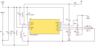
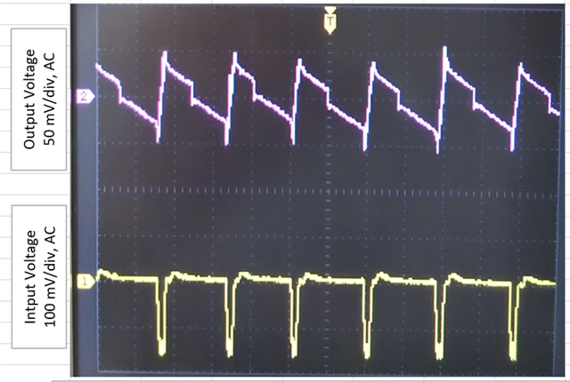
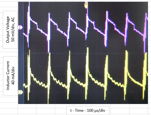
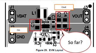
I designed the following circuit for our prototyping product.
In this case, the efficiency is too low.
Vin = 3V, Iin = 20mA, Vout = 5V, Iout = 8mA, Efficiency = 67%
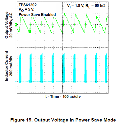
Power save mode = Enable
Do you think anything wrong to our circuit?
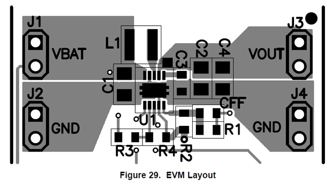
I designed the following circuit for our prototyping product.
In this case, the efficiency is too low.
Vin = 3V, Iin = 20mA, Vout = 5V, Iout = 8mA, Efficiency = 67%
Power save mode = Enable
Do you think anything wrong to our circuit?
