A related question is a question created from another question. When the related question is created, it will be automatically linked to the original question.
If you have a related question, please click the "Ask a related question" button in the top right corner. The newly created question will be automatically linked to this question.
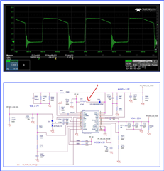
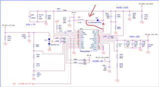
Connection of the switch node in your schematics is not correct. Switch node (pins 5 and 6) need to be connected to where you are pointing with the red arrow i.e. pins 5,6 should be connected at the junction of boost inductor and diode. Please refer to typical application schematics in the datasheet for proper connectivity.
This Schematics was wrong, and I reworked the board to have SW node (pins 5 and 6) connected at Diode Anode pin. The ring that I captured is there with the correct device application connectivity.
I don't see anything else wrong schematically related to this so I think that this ringing could be related to suboptimal board layout, especially given that you are blue wiring the switch node which has fast rise and fall times.