A related question is a question created from another question. When the related question is created, it will be automatically linked to the original question.
If you have a related question, please click the "Ask a related question" button in the top right corner. The newly created question will be automatically linked to this question.
When the charger is plugged in, Vsys is 3.65v (Vbat connects with 3.7V DC power supply); When the DC power supply is adjusted to 3.8V, Vsys measures 3.75V.
At this time, the register values as below:
When the charger is plugged into the USB port of the computer, it cannot charge:
CHG_ CONFIG:1
VBUS_ GD:1
IINLIM:8
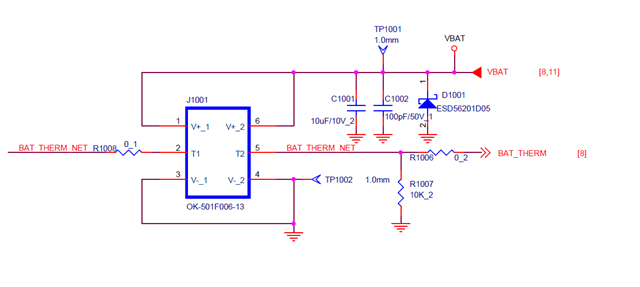
VBUS_ STAT: 1
When the charger is connect with a mobile phone charger, it cannot charge:
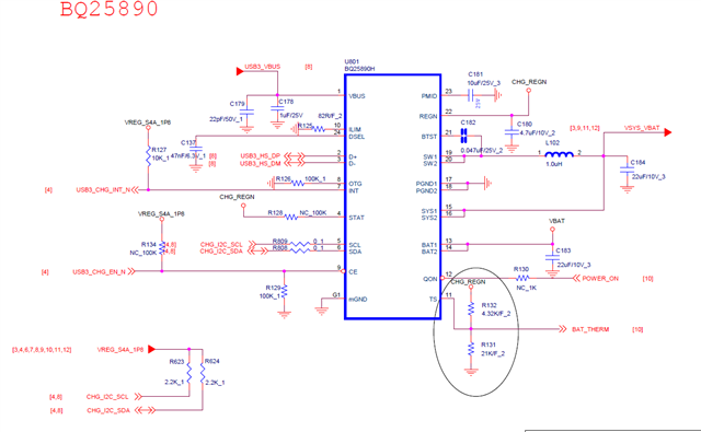
Taking a quick look I would double check the connections at a few pins, such as DSEL, but nothing stands out as preventing the device from charging.
Based on the additional information it appears the power supply at BAT is powering SYS, which is consistent with battery only mode operation. In charge mode Vsys should be larger than Vbat. Is the customer truly using a DC power supply for BAT? They need to use something such as a sourcemeter, which can sink current, as a battery simulator.
Can you please have the customer provide a full register reading so I can review all settings and statuses. Based on what is provided the device does correctly detect a good power supply with both "mobile phone charger" and "USB port" and sets the IINLIM accordingly (500mA for USB and 1.5A for charger adapter), but seeing the full status and fault registers would be helpful to conclude why no charge current is observed.