This thread has been locked.

If you have a related question, please click the "Ask a related question" button in the top right corner. The newly created question will be automatically linked to this question.

TPS53355: Loading ability confirmation

Part Number: TPS53355


hi team:

 My customer report the TPS53355 have two devices can not output 30A as usual, only 21A. But if the input voltage is increased, the output current capability will also increase.

 the situation of abnormal board is as below:

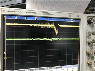
1.  5.5V input, 1V output, it is estimated to be about 21A.

2.  7.5V input, 1V output, it is estimated to be about 27A.

But normal boards, 5.5V input, 1V output, have about 27A..

 experiments we have try:

 1.The normal input is about 5.4V. If the input is raised to about 6V, other conditions remain unchanged, and the output load current can be increased by about 4A.

2. The first abnormal board adds an input capacitor of 200uF, the second abnormal board adds 300uF, and other conditions remain unchanged, the output load current can be increased by about 3A.

Basic inspection:

 1. No virtual welding, NO false welding.

 2. Using the fan to cold down. without over heat.

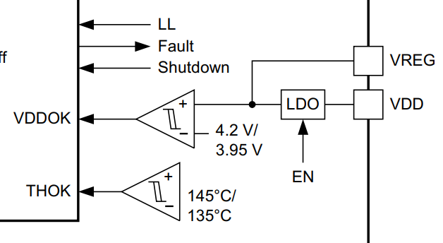
SCH upload as attached.

Can you help to review this SCH? And confirm why the above 2 experiment can increase the loading capability ?

 TKS in advance.

  • Hi Allen,

    Our US team will review it next Monday.

  • Hi Allen,

    Overall, the schematics look ok. However, I'm unsure about the multiple inductors at the output and if that's somehow preventing the full load capability.

    What load are you using to measure the loading capability, and what is happening at the switch node, etc., when the device stops supporting the load current? 

  • Hi Tomoya:

     tks for your comments, just work with customer to check more detail and waveform as you mentioned. I attached the file as below:

     And there is more detail i can share:

     1. VDD connect with VIN together, and i check the VDD/Vin when loading 28A, the min value is only 3.2V. the waveform of VDD shape just like the VREG one.

     2. 3.2V < 4.5V threshold of VDD, so the VREG will works on and off

     3. then the Vmode is jumping also, and the soft start time will go up and down

     4. and the VREG supply the internal logic control,  the output will works on and off

     5. the Vout seems backflow the PWM to the Vin.

     6. if use the oscilloscope to detect the Vfb ,the loading become normal , if may have something relate to the 2-10pf from the probe,

     7, i se the Rtrip as 240K as maximum value ,but on improvement,

    so i think the logic is as below :

     1.loading increase to 28A --> Vout jumps -->weak isolation internally--> noise backflow to the VIN--> VDD < 4.5V --> VREG works on and off -->

    LL work on and off -->Vout jumps


    based on the above experiments, would you have some advices?  

     TPS53355 waveform.docx

  • Hi Allen,

    Please ensure the power supply can supply 10 A DC current and the voltage at VDD is always above 4.5V. Otherwise, the converter will shut down as expected. It seems there is too much resistance in the input cable/trace (~200mΩ), so adding another cable would help.
    To confirm the VDD causing the issue, you can separately supply VDD and see if the problem disappears.

  • hi Tomoya:

     tks. we are trying to disconnect the VDD and VIN ,and use separate power supply to VDD , in order to keep VDD stable at first.

    It seems there is too much resistance in the input cable/trace (~200mΩ), so adding another cable would help.

    regarding this item, would you share how comes this summary?

  • Hi Allen,

    I estimated the input current to be about 5~6A based on their VOUT, IOUT, and VIN. If I understood correctly, the normal input is 5.4V, but the VDD measures 4.5V. Therefore, there is about a 1V drop from the power supply to VDD. 1V/5A gives 200mΩ. 

  • hi Tomoya:

     tks for your comments. 

     As i check with customer and have the below experiments:(separate supply VDD), the issue did not disappear.

    To confirm the VDD causing the issue, you can separately supply VDD and see if the problem disappears.

    the green is PIN19(VDD), the yellow one is PIN18(Vreg),as we can see , the VDD is higher than 4.5V but within a little ripple.

    but the Vreg output wIth a 1.67Khz ripple. have you seem this phenomenon? Or any experiments we can check? tks in advance.

  • attached the waveform of VDD=7V. other parameters do not change. And same issue occur.

  • Hi Allen,

    Please change the VREG capacitor to 16V rated or above. The DC bias loss of capacitance on a 10V cap operating at 5V output is severe and may compromise the stability of the LDO. 

  • hi Tomoya:

     Attached the waveform of VLL and Vreg with 50V 1uf cap of VREG capacitor, it seems nothing change.

    green is PIN6/7/8/9/10/11(VLL), the yellow one is PIN18(Vreg).

    is that okay that we can supply 5V to VREG  and float the VDD, that`s what we want to have a stable supply internally and check if it is the problem of LDO section.

  • Hi Allen,

    Yes, please try external 5V supply to VREG. 

  • Hi Tomoya:

     tks for your confirmation. I will this tmw.

     Besides, i did some additional tests today with customer with the abnormal board.

    1.  9Vin VDD, it can load 18A.

    2.  7Vin VDD, it can load 27A.

    3.  6Vin VDD, it can load 23A.

    4.  5.4Vin VDD, it can load 20A.

    5.  check with the OK board with Maximum 33~34A load, the LL waveform same as the below green one ,but the Vreg remain stable.

    Attached the waveform of VLL and Vreg with 50V 1uf cap of VREG capacitor, it seems nothing change.

    base on these experiments, i think there maybe something wrong with the internal LDO wafer.

    And different Vin may affect the efficiency of the LDO, this phenomenon is also in line with the characteristics of LDO. but check the impedance of the VDD and Vreg, roughly same as the OK one with 0.469V~0.55V.

    So i think it maybe the load capability of the LDO wafer, is there any inspection before the FA?

    Anyway, the external 5V of Vreg may help us troubleshoot the LDO problems.

  • Hi Ellen,

    Tomoya will review it and reply you by tomorrow.

  • Hi Allen,

    VREG LDO output voltage is inspected for test conditions up to 30mA.

    Please let us know if external 5V on VREG fixes the issue. If this resolves it, we can look into possibly improving the layout (e.g., location of the VREG cap, etc.).

    Also, is this the only unit exhibiting the issue, or are you seeing it on multiple devices?

  • Hi Tomoya:

     We found two devices have this issue. But due to the SCH ,VIN connect with VDD directly, supply 5V to Vreg need to cut the layout, so we are still considering.

     but just to want to confirm with you that why if external 5V on VREG fixes the issue, this issue is related to the layout problem? would you share your logic?

     As i see ,the VDD-VREG is a simple LDO in and out with internal enable function. if the separate VDD cannot fix and the external 5V on VREG can fix, i think this maybe the problem of the internal LDO.

     The another thing want to check with you is that the logic of UVLO.

     1. The VReg should output 5V as usual if the VDD is higher than 4.5V. why we need to check the stable voltage in this UVLO function? if there is any situation of the VREG will drop under the threshold?

     2. I think is more reasonable if the VDDOK detect the VDD voltage for UVLO.

    And below is the waveform of load transient for your reference.

    test condition: 1Vout,0-20A  load transient. LL in green and Vout in yellow.

  • Hi Allen,

    but just to want to confirm with you that why if external 5V on VREG fixes the issue, this issue is related to the layout problem?

    I wanted to look at the layout to ensure the VDD and VREG decoupling capacitors are placed as close to the device as possible. Poor bypassing on VDD or VREG can degrade the performance of the regulator.  

    why we need to check the stable voltage in this UVLO function?

    The voltage above UVLO is required for the proper operation of the converter. VREG can go below UVLO if VDD goes below 4.5V, but it could also drop if VREG is unstable or there is a short/overload condition on VREG.

    We found two devices have this issue.

    If you are suspecting this is due to quality issue, please submit it thru the customer return site on TI.com. 

  • Hi Tomoya:

     tks for your comments.

     today we exchange the device, and we found that the issue follow the faulty material. And new socket can work normally on the same board.

    But I put the faulty material into the OK board and the load capacity goes up to 25A. previously is 22A only. so i think there maybe the layout maybe affect too.

    As i attached the layout ,can you help to review of it? tks in advance!

  • Hi Allen,

    I noticed the VREG trace is going right underneath the LL node plane. This is OK if an inner GND plane is in between to shield and isolate from the LL node. 

    Also, the layout does not follow the following recommendation in the datasheet: 

  • hi Tomoya:

    I noticed the VREG trace is going right underneath the LL node plane. This is OK if an inner GND plane is in between to shield and isolate from the LL node. 

    As i check ,this trace is VIN+VDD。

    would you share the PCB files of EVM to my email? The details inside the EVM guide is hard to double check the trace.

  • Hi Allen,

    I just sent you the PCB files of EVM to your email. 

  • Hi Tomoya:

     tks for your email. I do want to update a new experiment with you. we try to welding this device into our EVM board. And it works well. 

    So I think there are still some factors that affect this device on the customer board. Is there a visual test to check the layout is causing this random problem?

     And we would like to test the Bode plot in next week.

  • Hi Allen,

    Good to hear the device works well on our EVM.

    For the visual test, you can check all the components and soldering are in good shape. You can check each pin/node with a multimeter and compare it with a known good board to see if there is a soldering bridge, etc.

    The layout guideline is in the datasheet. We also have an Excel layout checklist customers could use to review their layout: https://www.ti.com/lit/zip/sluraz7

  • Hi Tomoya:

    thanks for sharing. But I still want to know if we don't follow the layout, is there any tests to find out if it is caused by unreasonable layout?

    as we test the bode  plot ,i think it still shows good.

    1.EVM board:

    2. customer device1:

    3.customer device 2:

  • Hi Allen,

    Yes, there is usually a way to test if it's due to an unreasonable layout.

    For example, if we suspect it's due to the bypass cap placed too far away, you can usually put it somewhere closer by scraping off the solder mask on the board.

    If we suspect it's due to sensitive traces picking up noise, you can cut the path and reroute it on the board by having a wire across the board.

  • hi Tomaya:

     Do you think that  if we reroute it on the board by having a wire across the board will be more sensitive to pick up more noise?

  • Hi Allen,

    When you reroute it, you want to avoid the noisy area (e.g., SW node, etc.) and place the wire flat on the board, preferably on top of the ground plane for shielding. Try to keep the wire as short as possible.

  • hi Tomoya:

     tks for your always support!

     i sent you a email for further confirmation, would you help to take a look? tks!

  • Hi Allen,

    I saw your email, and I will continue to support you there. I will close this thread now since we transferred our communication over to email. Thank you.