This thread has been locked.

If you have a related question, please click the "Ask a related question" button in the top right corner. The newly created question will be automatically linked to this question.

LM5100A: LM5101A /B/C 3A, 2A and 1A High Voltage High Side

Part Number: LM5100A

Hi, we are now facing this issue.

In the part number LM5100A datasheet stated as below:

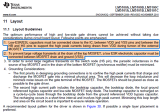
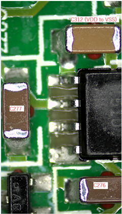
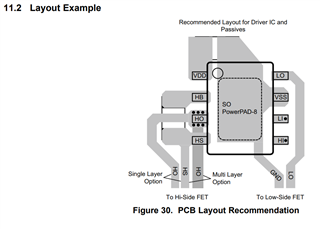
If the criteria that stated in the datasheet highlighted as below not meet, what is the impact and will it cause damage to the component with a low impedance path between pin 4 (HO) and pin 3 (HS)? 

  • Amira, 

    Welcome to the forum! Since the statements highlighted cover several recommendations, could you please clarify exactly which criteria is not being met? For example, do you not have these capacitors at all?, or you are using them but they are not low ESR?, or are you using all recommended components but they are not placed close to the pins as recommended in the layout?

    Best regards,

    Leslie

  • Hi Leslie,

    Refer to the image below, we have capacitors: C312 connected between VDD and VSS, C277 & C276 connected in series between HB and HS.

    Best Regards,

    Amira

  • Hi Amira, 

    Thanks for sharing the picture. The placement of VDD capacitor looks correct. Regarding the HB-HS capacitor, we recommend to place it as in the image below. What is the reason for having 2 capacitor is series from HB-HS? Typically there is only 1 bypass capacitor connected right at the HB and HS pins, or in some occasions with noisy environments customers might place an additional low value cap in parallel to filter high frequency noise. 

    The bootstrap cap is recharged every cycle from the VDD capacitor (through the bootstrap diode). This recharge occurs in a short time interval and involves high peak current so any long trace can cause parasitics that result in noise that might exceed the voltage that HB-HS can tolerate. 


    Regards,

    Leslie