This thread has been locked.

If you have a related question, please click the "Ask a related question" button in the top right corner. The newly created question will be automatically linked to this question.

TPS549D22: TPS549D22RVFR - X-ray unclean, voids are found

Part Number: TPS549D22
Other Parts Discussed in Thread: TPS548D22

Hi,

We met a question about below:

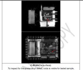
1. C-SCAN(Die surface): To inspect for the existence of defect, voids is visible for tested sample.

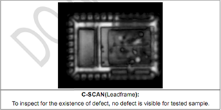
2. C-SCAN(Leadframe): To inspect for the existence of defect, no defect is visible for tested sample.

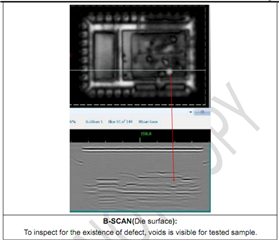
3. B-SCAN(Die surface): To inspect for the existence of defect, voids is visible for tested sample

Will this affect normal use?

Looking forward your reply

Thank you

  •  

    Thank you very much for the question.  What is pictured appears to be normal voiding in the solder die-attach between the MOSFET die and the lead-frame and clips.  It is expected.

    The TPS548D22 uses TI's Clip-Stack QFN packaging process where 3 separate die are co-packaged into a single multi-chip module (MCM).  The MOSFET die are "stacked" on the lead frame with the low-side FET directly on the thermal pad lead-frame.  The switch node clip is then stacked on the low-side die, followed by the high-side die and finally a PVIN clip.  Solder die attach is used to connect the MOSFET dice to the lead-frames and clips.  In order to prevent the solder from "doming" the amount of solder used is slightly less than 100% coverage, which result in some voiding at each interface.  The total amount of voiding, and the maximum size of any single void is monitored at the TI factories.

    This kind of small distributed voiding is typical and expected with the construction process.