Hi team,
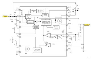
We designed a 12V to 40V boost converter using the TPS55332-Q1.
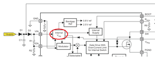
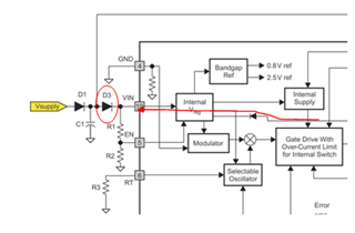
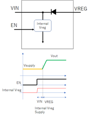
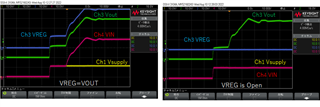
In the datasheet, there are D1 and D3 diodes in the functional block diagram.
Do our circuits also need them?
Best Regards,
Hi team,
We designed a 12V to 40V boost converter using the TPS55332-Q1.
In the datasheet, there are D1 and D3 diodes in the functional block diagram.
Do our circuits also need them?
Best Regards,