When selecting a MOSFET, there are two different types that can be considered for either a low-side or high-side switch. There are NMOS and PMOS MOSFETs to select from.
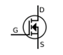
With an NMOS FET the source and the drain terminals are made up of n-type and a p-type substrate. When we apply a positive voltage to the gate of an NMOS MOSFET, electrons are allowed to flow from the drain to source.

Figure 1. NMOS MOSFET symbol
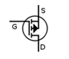
With a PMOS FET the source and the drain terminals are made up of p-type and a n-type substrate. When we apply a negative voltage to the gate of a PMOS MOSFET, electrons are allowed to flow from the source to drain.

Figure 2. PMOS MOSFET symbol
While the two seem to be opposite logics of one another, the implementation of the two in typical gate drive applications yield different considerations.
In a typical half bridge configuration, it is NOT recommended that we drive PMOS MOSFETs. Half Bridge gate drivers are designed to work with NMOS FETs on the high side and on the low side. There are a couple of issues designers can run into when placing a PMOS MOSFET in their design.
Designers can run into issues using a PMOS MOSFET when an UVLO event occurs. In most devices, when an UVLO event occurs, the outputs of the drivers are held low. When this logic is applied to a PMOS MOSFET, the MOSFET will conduct and act as a heating element which can cause it to burn up if current is running through it for a long enough time.
The majority of power supply applications utilize N-channel MOSFETs as the main power switch. TI suggest using a half-bridge driver if the PMOS is being used as a high-side FET in a half bridge, and replacing the PMOS with a NMOS. Using an NMOS MOSFET is beneficial in most designs due to the advantages of an NMOS over a PMOS.
Advantages of an NMOS:
- NMOS FETS are faster than PMOS FETs since the carriers are electrons rather than holes
- For an equivalent PMOS, an NMOS FET will have a lower on-resistance
- NMOS FETs have smaller solution sizes than PMOS FETs for the same complexity.
- NMOS FETs usually cost less than PMOS FETs
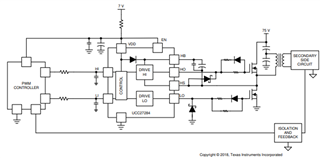
A simplified typical application diagram is shown below featuring UCC27284 which is TI’s latest half bridge driver switching an NMOS on the high and low side.

Figure 3. UCC27284 typical application
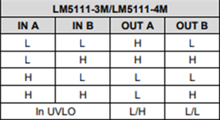
If using a PMOS is unavoidable, a solution that TI provides to this is the LM5111 which is a dual 5-A compound driver. The device comes in multiple variations such as -1, -2, -3, -4. The first three variations of the devices keep both outputs low during an UVLO event. The LM5111-4 is distinguished from the LM5111-3 by the active high output state of OUT_A during UVLO. When VCC is less than the UVLO threshold voltage, OUT_A of the LM5111-4 will be locked in the high state while OUT_B will be disabled in the low state. This configuration allows the LM5111-4 to drive a PMOS FET through OUT_A and an NFET through OUT_B with both FETs safely turned off during UVLO.

Figure 4. LM5111-4 truth table
For a more in-depth explanation of P-channel MOSFETs and gate drivers, please see the following:
Fundamentals of MOSFET and IGBT Gate Driver Circuits: https://www.ti.com/lit/ml/slua618a/slua618a.pdf?ts=1657747849290&ref_url=https%253A%252F%252Fwww.google.com%252F
For a link to the portfolio of TI low-side and half bridge gate drivers please see the following below:
Low-side: https://www.ti.com/power-management/gate-drivers/low-side-drivers/products.html
Half-Bridge: https://www.ti.com/power-management/gate-drivers/half-bridge-drivers/products.html

