This thread has been locked.

If you have a related question, please click the "Ask a related question" button in the top right corner. The newly created question will be automatically linked to this question.

TPS7A33: ESD protection method for the TPS7A33

Part Number: TPS7A33

Hi,

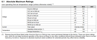
I am using TPS7A33 to generate -15 V from -16.5 V. The issue I met is the chip would fail consistently after a long term working. The output shows 0.65 V after the failure happen. In the data sheet, I found that the chip could be vulnerable to ESD issue, so I am planning to add a ESD protection circuit for the chip. My plan is to add a diode between the output and the ground. Hope to have your recommendation on ESD protection circuit and which diode model would work properly based on your experience. Thanks!

  • Hi Zeyu,

    If ESD is an issue then typically you will add a fast acting schottky diode that has a foward voltage drop of no greater than 0.3V.  This will prevent the voltage from exceeding the abs max rating in the datasheet.

    Thanks,

    Stephen

  • Hi Stephen,

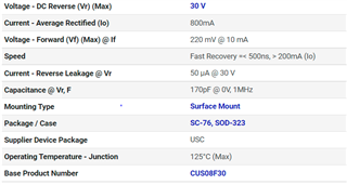
    Thanks for your reply. I found a fast recovery schottky diode CUS08F30, the spec shown as attached. Hope to have your suggestion.

    Best regards,

    Zeyu

  • Hi Zeyu,

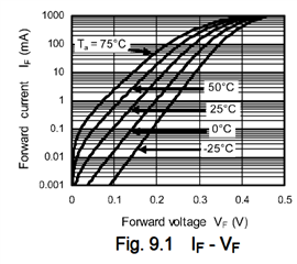
    This may work. The forward voltage will exceed 0.3V at higher currents and lower temperatures with this diode.  The linear regulator will rise in temperature and the schottky diode will also see some of this temperature increase, which will help you here.  This diode is a common footprint so if you need something else (and I'm not certain that you will) you can easily swap it out.

    FYI - I would be more concerned with the FB pin than the OUT pin, although you can try adding a diode to each.  The FB pin is typically the most sensitive node in linear regulators as it is unfiltered for the highest loop gain.  The OUT pin will have output capacitance, making a large ring or ESD event on that node unlikely (most ESD events do not have significant energy, thus they cannot charge up large amounts of capacitance.  But there is usually no capacitance on the FB node...).  As long as you are operating in something other than unity gain feedback (Vout > Vref) then the feedback resistors will prevent significant current flow through the diode, and this Vf should not exceed 0.3V.

    I'll quickly discuss the other pins: The NR/SS pin is similar to the OUT pin.  There is usually a large enough capacitor placed here to GND, and it is DC after turn on, so I would not expect this to be my most sensitive node to protect.  I would consider the EN pin as something to protect if you believe the ESD event can reach that node, and low capacitance is connected from there to GND.

    Thanks,

    Stephen

  • Thanks for your suggestion. I would also include ESD protection for the FB pin. In previous post I found that large reverse current for FB pin diode would mess up the output voltage. So I am wondering if you know how much reverse current would be safe for FB pin diode.

    Best regards,

    Zeyu

  • Hi Zeyu,

    Unfortunately we do not have the internal ESD pin diodes characterized to know those worst case reverse currents.  The feedback resistors should limit the reverse current into the FB pin, which will help.  And of course, the schottky diode will limit the voltage.  For these reasons, we are typically more worried about voltage stress on the FB pin than current.

    Thanks,

    Stephen

  • Thanks for your clarification. I am planning to use external diode CFSH05-20L TR PBFREE for FB pin protection. Hope to have your suggestion.

    Best regards,

    Zeyu

  • Hi Zeyu,

    I think the CFSH05-20L TR PBFREE would likely work for the FB pin.

    Thanks,

    Stephen