This thread has been locked.

If you have a related question, please click the "Ask a related question" button in the top right corner. The newly created question will be automatically linked to this question.

TPS23754EVM-383: PD can't output normally when PSE plug in(TPS23754)

Part Number: TPS23754EVM-383
Other Parts Discussed in Thread: TPS23754,

Hi

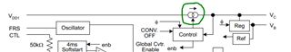
It's old bug. I had ever raised the issue on TI forums. Please help to review the website:

https://e2e.ti.com/support/power-management-group/power-management/f/power-management-forum/1112016/tps23754-pd-can-t-output-when-pse-plug-in-tps23754

Barbecue S PD board.pdf

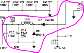
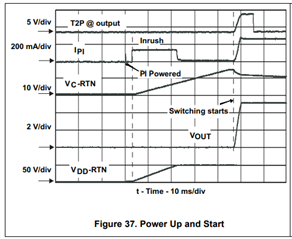
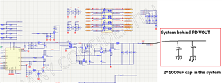
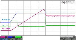
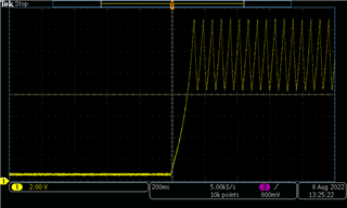
The defect rate of new PCB is higher than previous version >> VOUT is no output (15V).

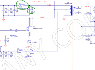
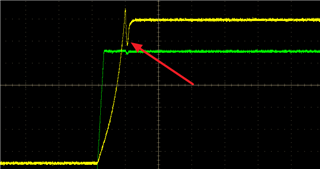
We found that changing C89 from 22uF to 1uF could improve.

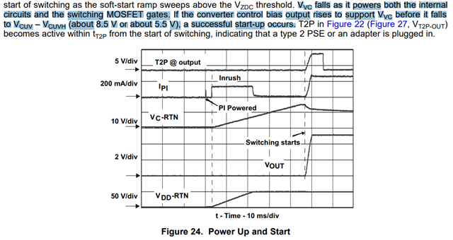
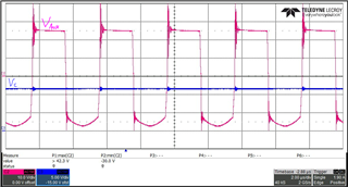
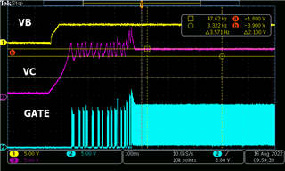
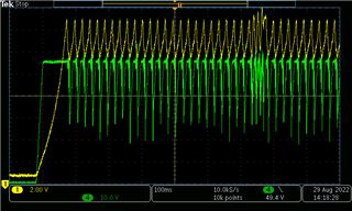
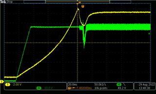
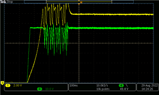
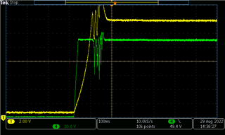
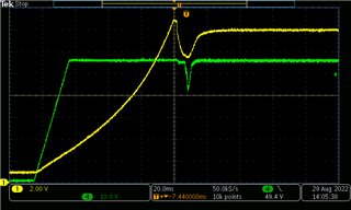
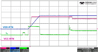
Below is VCC waveform.

C89=22uF

C89=1uF

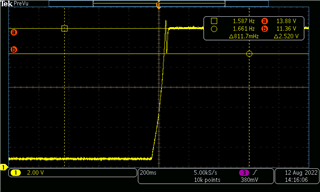
Could you help to explain why reduce the soft-start capacitance can improve VCC waveform?

Thanks

Wendy

  • Hi Wendy,

    Thanks for your question and glad to hear you improved V_C voltage ringing!

    Here is my guess: Before the converter work or when the V_CTL is below 1.5 V, the duty cycle is 0%. C89 with 22uF results a long ACF converter feedback control delay time. Then both the V_CTL and the duty cycle need a longer time to reach the steady state value (rise speeds are slow for both). Since the V_C capacitors (C83, C84, C94) can only be charged when U25 is on, however the on-time of U25 is limited by the low duty cycle at start-up, you may not be able to drain enough current from transformer winding 4-5 in each switching cycle.

    Best regards,

    Diang

  • Hi Diang

    1. Please see VC waveform I attached last week,the stable voltage is 13.88V. Is it normal? 

    2. Which component of PD circuit would also  effect VC. 

    3. Below picture is trandformer spec.Please help to check is the spec suitabble and tell me which is important parameter? (VOUT of my design is 15V)

    Thanks

    Wendy

  • Hi Wendy,

    1. The max voltage between VC to RTN is 19 V. But according to #3, I felt the transformer selection could be a problem.

    2. For TPS23754 in the ACF converter topology, I would say the turns ratio between PRI and AUX takes the major effect. 

    3. This transformer picture looks like a flyback transformer (a coupled inductor). I do not think it is suitable for ACF converter in your schematic. For flyback converter case, normally the 12-V AUX winding only conductible with its VC capacitor when the 15-V SEC winding is connected with the load capacitance bank (as shown below). Could you send a full version datasheet of your transformer?

    Best regards,

    Diang

  • Hi Diang

    Below is transformer spec.

    LDT6085-50R_SPEC_A.PDF

    Our PD circuit is ACF ,which followed TPS23754EVM-383 EVM's circuit. And transformer is Forward Transformer.
    Forward Transformer


    Could you provide the spec of the turns ratio between PRI and AUX for TPS23754 ACF circuit.

    Wendy

  • Hi Wendy,

    Thanks for the datasheet!

    The voltages marked on the windings are not the same with the effective turns ratio, which makes me feel it is a transformer for flyback converter (e.g., PIN 1-2 turn: PIN 6,7-9,10 turn = 1.40; but PIN 1-2 voltage : PIN 6,7-9,10 voltage > 2 ). But after seeing the datasheet, I believe it is forward transformer. 

    I just measured a FPS23730 EVM which is ACF with the transformer information shown below.

    With 50-V PoE input voltage, 2:1 PRI to AUX turns ratio, the AUX winding voltage is between +1/2*V_poe and -1/2(V_Clamp - V_poe), and the AUX voltage shares the same duty cycle of the main ACF power circuit. With diode D7 the half-wave rectifier, the circuit to output V_C is like a bulk converter.   


    With a sufficient L3 inductor, the AUX circuit should be continuous mode. Then using the Bulk converter formula and ignoring the diode forward drop, the V_C voltage should be

    V_C = [V_poe / (N_PRI : N_AUX) ]  * D

    Then the V_poe, turns ratio, and duty cycle will influence V_C.

    A large C89 will make the duty cycle (D) at a low value for a longer time at the start-up theoretically. In that case, I would suspect the duty cycle D could be more unstable (or varying) at start-up. Since the V_C's load is V_B, and V_B is used for duty cycle control, and the duty cycle will influence V_C. Some disturbance may occur in this loop and cause your V_C oscillation.

    Best regards,

    Diang

  • Hi Diang 


    Thanks for your explanation.


    We found that the capacitance quantity of system also would effect the PD output.

    Plaese see below picture. It seems VB is no problem. VC & GATE are un-normal.

    Do you know How to slove the issue with high capacitance loading? Or Add VC bypass capacitor is the only one solution?


    Thanks.

    Wendy

  • Hi Wendy,

    Thanks for your test. 

    "We found that the capacitance quantity of system also would effect the PD output." May I know which capacitance do you mean?

    For the voltage of V_C, the initial rise is caused by the internal current source inside the TPS23754. When it reaches 15 V, the DC/DC converter starts work and the voltage of V_C is contributed by output voltage of that Buck converter in AUX winding. We saw the oscillation after the 15 V is reached. So this problem should be related to the Buck converter start-up. 

    Since AUX winding voltage is related to the PRI winding coupling. At that start-up, the 1-uF C72 and 3.3-uH L27 could cause some voltage oscillation at PRI winding. So I would suggest to increase the C72's capacitance to ~10 uF, or try without the L27.

    Best regards,

    Diang

  • Hi Diang

    I mean that PD supply 15V for our system and there are big capacotor in our system.

    I reduce the quantity of capacitor from 2 to 1, the VC waveform would be improved.


    (CH1: VC,CH2:PVDD-RTN)

    left waveform : system use 2*1000uF                                                         right: system use 1*1000uF


    I tried add C72 and also tried to remove L27

    left waveform : add C72 from 1uF to 3*1uF                                                        right: without L27


    add C72 from 1uF to 5*1uF and system use 5*1uF

    The VC and PVDD-RTN seems better than original design,but the drop of VC stilll exist.

    Wendy

  • Hi Wendy,

    Thank you for your test! I measured VDD-RTN and Vcc-RTN with TPS23754EVM (5-Vout version) and TPS23730EVM which are both ACF circuits. Both have a voltage drop at Vcc  when DC/DC starts to work. For the TPS23754EVM (5-Vout version), after the drop it stayed at ~10.5 V. 

    Since, V_C = [V_poe / (N_PRI : N_AUX) ] * D, and V_OUT = [V_poe / (N_PRI : N_SEC) ] * D

    We should have V_C = V_OUT * (N_AUX / N_SEC). 

    Adding 1000 uF cap moved the Vout pole to a lower frequency and may influence V_OUT, then V_C got influenced. So does changing C89 which changed the V_OUT. Could you measure your Vout and Vcc with differential probes? Probably when Vout gets more stable at startup, Vcc can also be improved. 

    TPS23754EVM (5-Vout version) test: C_Vcc = 23uF, V_OUT = 5V, N_AUX / N_SEC = 2.36

    TPS23730EVM test: C_Vcc = 1 uF, V_OUT = 12V, N_AUX / N_SEC = 1

    Best regards,

    Diang