This thread has been locked.

If you have a related question, please click the "Ask a related question" button in the top right corner. The newly created question will be automatically linked to this question.

MC33063A: Inverting Converter Application Component Selection and Operation

Part Number: MC33063A

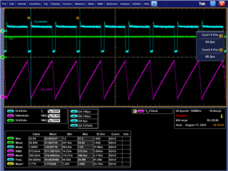
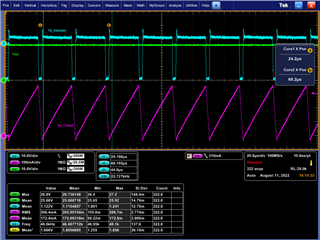
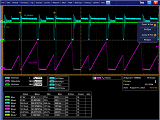
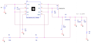
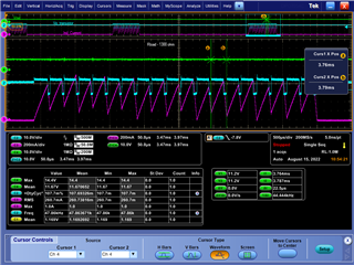
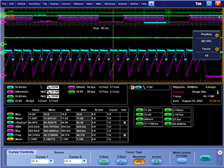
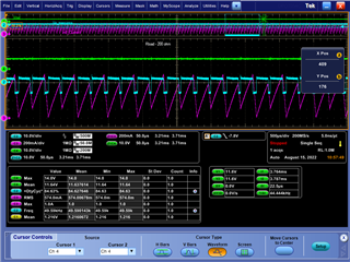
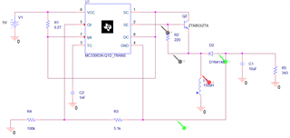
                I am trying to put together a design, using the MC33063A IC, and I’m having some trouble getting it to function properly on the bench.  I am trying to use the chip in an inverting regulator setup, with an external npn switch to create a -25.75V rail @ 75mA of output current.  Below is my schematic (R5 is the load of the converter – set to draw 75mA at -25.75V).  When I simulate this, I get the correct output regulation, but when I build it on my bench, it will only regulate properly at very light loads.  At any load with a resistance below about 2.3kohm (about 11mA), the output voltage gets pulled lower and lower.  I attached a few plots to show what I’m seeing - they are at 6300 ohms, 2300 ohms, and 1300 ohms of resistive load (R5 in the schematic).  It seems like I’m hitting some sort of power limit when the inductor is no longer in discontinuous mode, but I can’t figure out exactly why it's happening, or what is wrong with my calculations.  I’ve tried reducing R1 to a lower value with no effect.  I’ve tried multiple Ct caps with no effect.  I don’t think I’m violating any electrical ratings on the diode or npn transistor.  The inductor is rated to 1A peak, and I’m not getting close to that.  Any assistance you can offer would be appreciated.  Thanks.
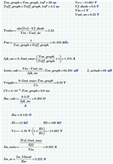
Below is my design equations for component selection.  It follows the equations listed in 9.2.1.2 in the https://www.ti.com/lit/ds/symlink/mc34063a.pdf datasheet.
  • Hello Joe,

    Thanks for reaching out to us via e2e.
    I will have a look at your questions, but as Monday will be a bank hoiday it may take until mid of next week until I will get to it.

    Best regards,
    Harry

  • Hello Joe,

    I have observed three things:
    - The chosen switching frequency is very low.
            It should be around 100 kHz.


    - The output capacitor is way too low.
            It should be minimum 330 µF, the datasheet even shows 1000 µF

    - There is no input capacitor at all.
            Even if the datasheet shows 100 µF, I would also propose a bigger capacitor (up to multiple 1000 µF) on the input side. This depends on your supply.

    In general it is good practice to place maybe 10 µF ceramic caps as close as possible to the input pin and rectifier diode and use big aluminium electrolytic caps with low ESR right behind those.

    Best regards,
    Harry

  • Harry,

    Thanks for the reply.

    For the switching frequency, I didn't think there was anything it *should* be (though I did try running at 100kHz, and got very similar results).  I am trying to replace an existing design (which uses the New Japan Radio 2630D chip) that runs around 50kHz, so I just tried keeping the switching frequency around there.  In the reference design in the datasheet (figure 8), a 1.5nF cap is shown for the Ct pin, which would give an even lower frequency than my design.  The inductor value I picked was calculated based on that ~41kHz frequency.

    For the output cap, I'll take a closer look.  10uF was what was used on the previous design, and I just copied it over.  The output rail looked pretty solid with just the 10uF aluminum electrolytic cap I had, but it's easy enough to put a 1000uF cap there and see if anything improves.

    I do have input capacitance of several hundred uF; I just didn't model that in my simulation since I was using an ideal voltage source for the rail.

    On the plot that has the uneven inductor current - is that supposed to occur?  Or is it indicative of something I should look closer at?  I don't know why some cycles have only about half the on-time as the others.

    Thanks,
    Joe

  • Hello Joe,

    Today is a bank holiday for us.

    For the input / output caps, please make sure that you will use a combination of ceramic caps and low ESR + low ESL aluminium electrolytic caps.

    Best regards,

    Harry 

  • Hi Joe,

    It is possible that the max duty cycle 80% is reached. You will have a higher gain at DCM compared to CCM. You may reduce the inductance to check if it helps.

    Best Regards,

    Feng Ji

  • Feng,

    Thanks.  Reducing the inductance definitely helps.  I had tested that last week, too.  My concern was the mismatch between the value I'm using on the bench, and the value I get in the calculations from the equations in 9.2.1.2.

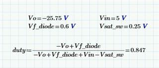
    The max duty cycle limit wasn't something I considered.  I didn't see anywhere in the datasheet that listed 80% as a max, and I am going to need higher than that:

    That's with a nominal in and out voltage.  With tolerance factored in, it gets to maybe 88%, worst case.  Can you point me to where a max 80% is listed?

    Thanks,
    Joe

  • Hi Joe,

    I read it in the product folder.

    https://www.ti.com/product/MC33063A

    Best Regards,

    Feng Ji

  • Thanks - I did not look in the product folder.

    I imagine that's the issue, then.  I'm going to retool my design to not jump straight to -25.75V.  The full application has multiple output voltages that I'm generating through a transformer.  I can just add a winding that regulates to a lower voltage, and set the transformer turns ratio to get me -25.75 where I need it.

    I'll update my breadboard design today with this, and close out this issue, assuming it is resolved.

  • Unfortunately, these changes didn't really fix my issue.  Here's my updated schematic:

    I've added a bunch of output capacitance - 1500uF aluminum electrolytic and 10uF ceramic.  I still have a bunch of input capacitance - it's just not in the simulation pic.

    I decreased the regulated voltage to -11.667V instead of the previous -25.75V.  My needed output current is now 128mA, which equates to a ~91 ohm load.

    I kept the switching frequency around 45kHz, and lowered the inductance to 68uH.  That's the value I get 

    I'm still getting weird switching waveforms:

    At  Rload=1300 ohms (roughly 9mA), I get a kind of burst mode, where the converter runs for several cycles, then turns off for a while, and repeats.  When it's on, it looks like it is running at max duty cycle, and the inductor current looks unstable.  It looks like the

    At Rload=300 ohms (roughly 39mA), I get the same thing, but the time between bursts is decreased.  If I leave it running in this condition, the input current starts creeping up - something is getting into a thermal runaway, I assume, but I didn't leave it on long enough to see.

    At Rload=200 ohms (roughly 58mA), there stops being bursts, and it runs in this mode continuously.  The input current quickly rises, and I don't want to leave it on for more than a maybe 10 seconds.

    I've also read through sections 4 and 5 of https://www.ti.com/lit/an/slva252b/slva252b.pdf, but it isn't helping me understand what I'm doing wrong.

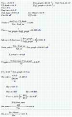
    Updated design equations below:

    Thanks,
    Joe

  • In case it helps, I get the same behavior if I don't use the external switch - it's even a bit worse, in fact.  I removed Q2 and R2, and then tied pin 2 of the IC to the cathode-inductor net.  I also tried multiple inductances from 68uH to 150uH, with no real improvement.  At light load, I regulate just fine, but at some point, it looks like the inductor current starts to ratchet up, Iin starts rapidly increasing, and I have to shut of the 5V input for fear of causing something to smoke.

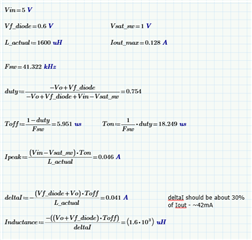
    Could I get a second set of eyes on my design equations to make sure I'm understanding how the chip wants me to calculate desired inductance?  I'm getting the feeling that I'm incredibly low.  If I use a method to calculate inductance that's agnostic of the MC33063a chip, I get something closer to 1600uH:

    Thanks,
    Joe

  • Hi Joe,

    In slva252b, it is suggested to have the converter in DCM (BCM for full load), that means the ripple factor will be 200%.

    30% is a reasonable ripple factor for CCM, but please note that the ripple factor should be (ripple current) / (inductor current), not (ripple current) / (output current). This result in a larger inductor in your calculation.

    Best Regards,

    Feng Ji

  • Hello Joe,

    We have not heard from you for a while, so I assume your problem has been solved and I am closing this thread now.
    You can re-open it or simply start a new one if this one got locked.

    Best regards,
    Harry