This thread has been locked.

If you have a related question, please click the "Ask a related question" button in the top right corner. The newly created question will be automatically linked to this question.

UCC27211: The Ringing in the MOSFET using the UCC27211 as the gate driver in 4 Switches Buck-Boost Converter

Part Number: UCC27211

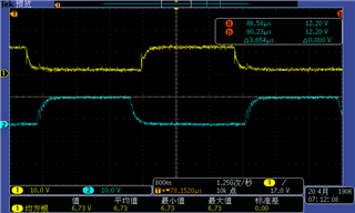
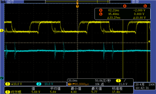
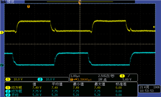
Hi, I used UCC27211 as the gate driver in 4 Switches Buck-Boost converter.

When the converter works in boost mode, there are a big ringing reflected to the upper MOSFET as the lower MOSFET turn on. What is the reason of this big ringing? Besides, this ringing will also affect the output.

Vgs waveforms(Yellow: Upper MOSFET)  Vgs(upper) and output

  • Hello Yishan,

    Ringing that is seen on one Mosfet in a power stage when the other Mosfet switches is usually from the Mosfet Vds slew rate and the Miller charge which will be injected into the Mosfet gate to source. I assume the waveforms shown are the Mosfet gate drive signals. One way to reduce the amount of ringing is to reduce the dV/dt by adjusting the gate resistance between the gate driver output and Mosfet gate. 

    Regards,

  • Thank you very much for your reply, figure 1 is indeed the gate drive signals. The following figure is more clearer. I have tried different resistance from 5 to 27ohm but this ringing is still exist and evident.

  • Hello Yishan,

    One thing that can help to control the dV/dt of the switching events and also provide some attenuation of the Vgs perturbations from dV/dt, is to have a higher turn on gate resistance and a diode and smaller resistance in parallel for lower turn off resistance. 

    Another way to reduce the voltage disturbance on the Vgs waveform, especially if the gate drive traces may be a little long, is to have a capacitance from gate to source close to the MOSFET gate and source pins. This will reduce the Vgs disturbance from the miller charge during switching.

    Regards,