This thread has been locked.

If you have a related question, please click the "Ask a related question" button in the top right corner. The newly created question will be automatically linked to this question.

UCC2897: 12V/11A

Part Number: UCC2897

Hi

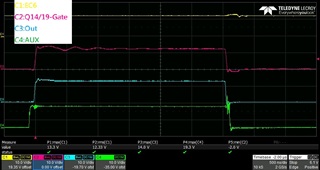
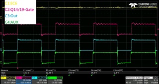
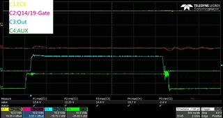
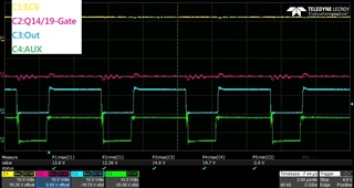
Customers can adjust RDEL from 4.99KΩ to 5.6KΩ and 10KΩ according to the Spec,

and the measurement waveform is as attached It is found that when the Q14/Q19 is adjusted to 10K,

there is no signal to turn it on. How can I adjust it?

P4 schematic.pdf

  • Hi Gareth,

    Thanks for connecting through E2E. One thing to note about changing the value of RDEL is the relationship this has against LINEOV and LINEUV and I've highlighted in the block diagram below:

    As you change RDEL, the value of IRDEL is changing which is moving the set point for LINEOV and LINEUV. I believe when you changed RDEL to 10 kΩ and saw no output, you most likely entered LINEUV protection. If you need the amount of delay corresponding to RDEL=10 kΩ, be sure to adjust the LINEUV, LINEOV resistor dividers accordingly. Since you have RDEL=10 kΩ installed and you are not seeing any output, you should be able to vary the input voltage while monitoring LINEUV, LINEOV against the 1.27 V threshold. Adjust VIN so that LINEUV, LINEOV are less than 1.27 V and you should see the output switching...ultimately you need to set the LINEUV, LINEOV resistor dividers correct according to your final chosen value of RDEL.

    Regards,

    Steve M

  • Hi Steven

    Thanks for the detailed explanation

    Because the 12V input draws more than 8A, the temperature of Q12 will be close to 200 degrees
    In order to solve this problem will increase the delay time of Q12 and Q14/Q19 so that they are not turned on at the same time

    But how much RDEL must be adjusted to be enough delay time?

  • Gareth,

    You need to set the dead time so there is enough time for VDS to resonate to to zero at full load. As you decrease the load you should observe that the VDS may not full resonate to zero but only reaches some minimum value. In other words we lose ZVS at some minimum load current but the condition we care most about is setting the dead time just long enough to observe ZVS at minimum input voltage, full load current. You can calculate the required time to fully resonate VD to zero at full load but this requires a thorough understanding of the total resonant current flowing in the primary and the total resonant capacitance we are trying to discharge. If you don't feel you can work through the calculations, you can arbitrarily set a dead time on the bench and make the adjustment on the fly. 200°C seems to hot for your primary MOSFETs. What does your VGS, VDS look like - is the clamp capacitor resonating correctly and if so, you should see a slightly rounded top on the VDS that is equal to ~20% VDS ripple. From SLUA535A, you can see that in addition to RDEL related to LINEUV and LINEOV setting, it also impact the max duty cycle clamp. One thing you might check it try slowly decreasing VIN while monitoring the duty cycle - when you reach VIN=12V is the max duty cycle clamp active - Can you go below 12V and still see the duty cycle increasing? If VIN=12V is hitting your max duty cycle clamp, you should see your output voltage start to drop. Measure the duty cycle at 12V and assure yourself it's what you intended.

    Regards,

    Steve M