This thread has been locked.

If you have a related question, please click the "Ask a related question" button in the top right corner. The newly created question will be automatically linked to this question.

TPS65263-1Q1: Please review the schematic

Part Number: TPS65263-1Q1

Hello TI experts,

My customer drew their first schematic with TPS65263-1Q1. Could you review the schematic?

and here are some questions.

1. They don't want to use I2C communication for setting.

Is it okay to set ENx pin floating to enable each DCDC module output, and SDA/SCL also floating for not using??

2. what would be happen if ENx is pulled up or pulled down?

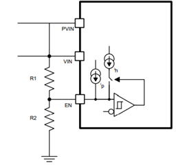
3. If we want to adjust the input UVLO through ENx pin, is it okay to design schematic like this?

(cause we don't want to use I2C communication, and we have to float ENx pins in this situation.)

4. please also check feedback resistor of the schematic above.

Best regards,

Chase

  • Hi Chase,

    My colleague Lucia will give you response by Monday when she comes back to office!

    BRs

    Zixu

  • Hi Chase,

    Thanks for reaching out! Sorry for late response. For the questions,

    (1) If customer don's use I2C,  please leave SCL and SDA pin floating. It's okay to set ENx pin floating to enable DCDC.

    (2) If ENx is pulled up and EN voltage is above EN threshold, the device will be enabled. If ENx is pulled down, it will be disabled.

    BRs

    Lucia

  • Hi Chase,

    (3) I have checked the schematic. Will R11 and R10 not mounted? If customer want to adjust UVLO, it's not okay to just float ENx. Please refer to the circuit shown below to adjust UVLO. The resistors R11 and R10 are still needed which means EN can not just leave float.

    (4) I am good for the resistor.

    Anything unclear, please kindly let me know. Thanks!

    BRs

    Lucia