This thread has been locked.

If you have a related question, please click the "Ask a related question" button in the top right corner. The newly created question will be automatically linked to this question.

TPS74801: CS1238727

Part Number: TPS74801

Hi,follow picture is about my design of TPS74801。

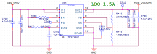
yesterday,I want to test whether the load of PCIE_VCCA2P5 can withstand 2.5+-10%,so i set the LDO do not work by tie the PIN5 EN to GND。

After i complete the test,recover the connect style of PIN5 EN to enable the TPS74801 to work。

I power on,the output of TPS74801 is 4.2V not 2.5V.The voltage of the PIN8 FB is 0V.

I DON'T know what the problem is.

  • Hello, 

    Are you testing out this connection on a populated board or just in PSPICE?

    Comments on the schematic:

    - When Bias is connected to VIN, the CBIAS value must be 4.7uF.

    - If using the PG pin to monitor the output voltage, the pin must be pulled up with a resistor. 

    - A 5V input to 2.5V output with a 1.5A load will lead put the part into thermal shutdown (if using the JEDEC standard PCB layout and the VQFN package) by 35C ambient.

    If it is only in PSPICE, have you checked to see if R1 is connected?

    Best,

    Juliette