This thread has been locked.

If you have a related question, please click the "Ask a related question" button in the top right corner. The newly created question will be automatically linked to this question.

TPS61372: separating device powering (Vin) from main boost power flow

Part Number: TPS61372

Hi,

I want to try and use the  TPS61372 with energy bank going as low as 1.2V while keeping stable output voltage of 12V@0.3A.

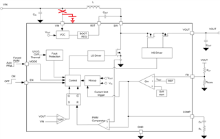
For this I would like to separate the input voltage of the device (Vin) and the main boost power flow.

Vin will be powered by external low power 5V. I simulated it and the output stabilized on 5V instead of 12V.

I did noticed that in the block schematics the Vin is used by the control of output voltage, and the question is if there a way to go around it?

  • Hi Zeev,

    I check the simulation model and it shows no problem like you mentioned.

    please refer to this.

    https://e2e.ti.com/cfs-file/__key/communityserver-discussions-components-files/196/TPS61372_5F00_PSPICE_5F00_TRANS.7z

    It is viable to separate the input voltage of the device (Vin) and the main boost power flow.

    Please connect the EN pin to main power flow or control it after the power is on.

    When connected to Vin pin, the voltage may not enough to reach threshold  and  there maybe premature switching before power on.

    Thanks 

    Fergus