This thread has been locked.

If you have a related question, please click the "Ask a related question" button in the top right corner. The newly created question will be automatically linked to this question.

LM5123-Q1: Strange behavior of low-side-FET gate

Part Number: LM5123-Q1

Hi!

The following observations have been made with a pre-production-sample of the LM5123 (XLM5123). If this is a known issue and it is fixed with the production version, please let me know.

While measuring our design, we found an unusual behavior of the gate of the low side transistor, connected to "LO" on the IC.

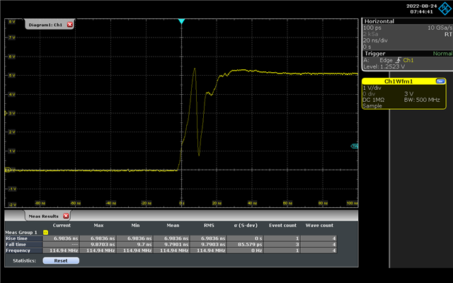
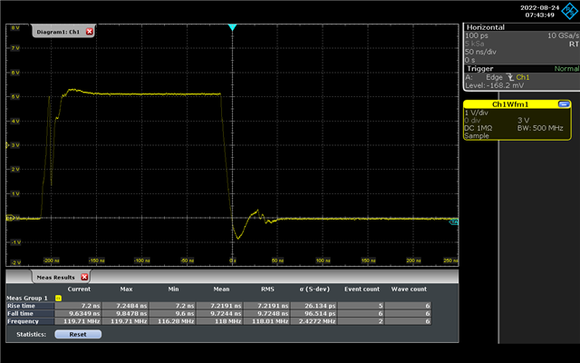
The gate driver voltage seems to break down while initially supplying the gate. The following oscilloscope measurements were made between gate and source (GND) of the low side FET, with a very short ground lead on the probe.

Close-up of rising edge:

Complete cycle of the lowside FET:

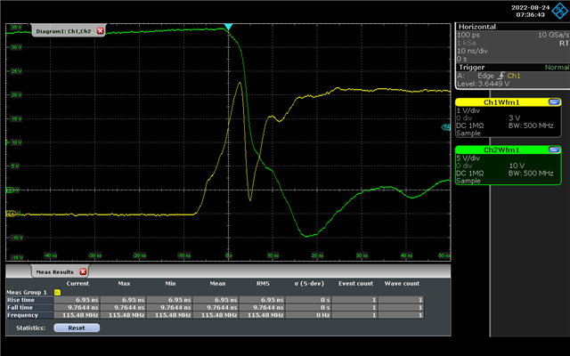
The next image shows the switch node in green for reference (values there might not be exact because the ground reference is on the other probe)

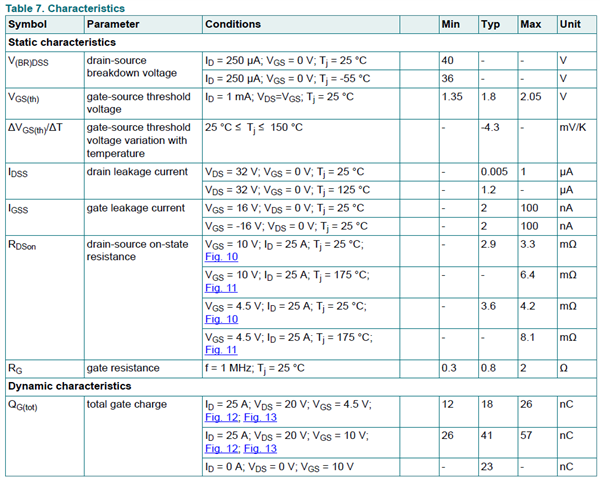
We are using the Nexperia PSMN3R2-40YLD, which has the following characteristics:

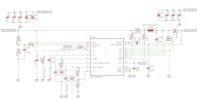
This is our schematic

The lowside FET gets relatively warm, we assume this is because the gate takes a long time to fully charge, and therefore the FET is in linear mode for longer than needed.

Can you provide us any information on this behavior? Is there anythin we can do to improve performance?

Best regards

Felix

  • Hello Felix,

    Thanks for reaching out to us via e2e.

    This ringing is not an issue of the early devices.

    There are at least two options how this problem can be generated:

    1) A fast switching FET will cause ringing
    Try to slow down the switching of the FET by adding a gate resistor and an RC snubber in parallel to the low side FET.

    2) Layout considerations
    Please make sure that you are closely following the layout guidelines in section 11 of the datasheet.

    Keep the high current loops as small as possible. Connect the gates via short solid traces.
    Keep the controller outside of the "noisy" area.
    Take special care of the Ground:
    Keep AGND and PGND separate and only connected at one common point
    Keep the GND of the input separate from the GND of the output loop.
    Ideally follow the example shown in chapter 11.2. of the datasheet. As you can see, there is no solid ground plane.
    The layout guidelines are not just a proposal. It is a strong recommendation to follow all the rules listed in the datasheet to make the design work properly.

    Best regards,
    Harry