This thread has been locked.

If you have a related question, please click the "Ask a related question" button in the top right corner. The newly created question will be automatically linked to this question.

UCC28950: ucc28950 senkron rectf. snubber question

Part Number: UCC28950

Hello,

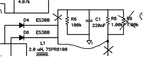
My snubber circuit in the picture, its temperature increases too much as the output load increases, I think its values are wrong,
what is the reason.
how do I fix it,
is the calculation document available?
Best regards

  • Hello,

    I could not find equations on how to setup this RCD clamp on TI's website.  This RCD clamp looks like it was trying to recover the leakage stored in the clamp capacitor.

    You may want to try a tridiagonal RCD clamp instead.  Instead of connecting R8 and R9 to the output you could tie them to the anode's of D4 and D6.

    You could possibly get rid of R9  I marked up the schematic below.


    The voltage stored across C1 = Vout*2.  I think R6 and C1 at 100 k and is a good starting point.

    R8 is set to clamp the maximum SR FET Vds voltage (Vdsmax).  I would recommend setting to 80% of the FETs maxim FET voltage.

    You should be able use the following equation.

    R8 = (Vdsmax*0.8 - VD6 - Vout/2)/Iout

    Voltage cross R8 when clamp is active:

    VR8 = Iout*R8

    Diode D4, D6 and R8 will dissipate all of the leakage energy from the secondary leakage inductance (Lslk).

    The following equation will estimate the power dissipation of the leakage inductance (Pslk).

    Pslk= ((Lslk/2)*(Iout)^2)*fsw

    The following equations can be used to estimate VD4, VD6 and VD8 losses.

    VD4 = 0.8V

    PR8 = Pslk*VR8/(VR8+VD4)

    PD4=PD6= Pslk*VR8/(VR8+VD4)

    The power dissipated in R6 = ((Vout*2)^2)/R6

    Regards,

  • Hello,

    If the value of the L1 inductor is chosen small, does it affect this situation?, Is there a factor other than "Llk" that creates this energy?

    Regards

  • for example, I calculate my "TEFSET" value as 32 nS, it's actually a little small

  • Hello,

    If the output inductor (L1) is chosen small you will have more inductor ripple current and higher peak inductor current.

    The clamp  discharging the energy in the transformer's secondary side leakage inductance (Lslk) when the SR FET turns off.  It is not trying to clamp the energy in the output inductor (L1).  However, the peak current in Lslk will be the same as L1.

    The more I think about this when choosing R8 you size it based on the peak inductor current (IL1max).  The following equation should help.

    R8 = (Vdsmax*0.8 - VD6 - Vout/2)/(IL1max)

    Regards,

  • Hello,

    where does "Vout/2" come from in the formula below?

  • Hello,

    That is a mistake it should be Vout*2 and not Vout/2.   The clamp circuit is used when the FET turns off.  The voltage across the winding that is on is the same as the one that is off.  That means the voltage at the winding that turned off without the leakage spike is 2*Vout.

    Regards,