This thread has been locked.

If you have a related question, please click the "Ask a related question" button in the top right corner. The newly created question will be automatically linked to this question.

LM74502Q1EVM: OV behavior during and after OV in cutoff mode

Part Number: LM74502Q1EVM
Other Parts Discussed in Thread: LM74502-Q1, LM74502, LM74502H-Q1, LM74502H,

Hello Team,

We are trying to evaluate the LM74502-Q1 as a over voltage protection. Testing the OV cutoff behavior on the Q1 EVM we see the following behavior. It doesn't look to be intended behavior and debugging so far doesn't give any clue on the root cause.

  1. OV threshold is set to 36V
  2. Going from normal operation above 36V behavior is as expected and output turns off
  3. Decreasing Vin then slightly below 36V gives the behavior we see on the scope shot
  4. Decreasing Vin further to below 28V the behavior is again as expected and output is on

So far tests have been made without inrush current control and behavior was fine at first. Now with this behavior observed only adding the RC for inrush current control fixed the "issue".

Attached some scope plots.

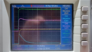
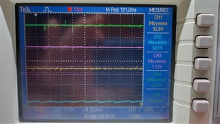
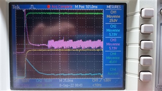
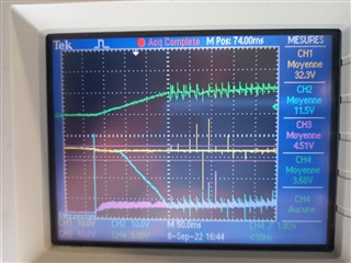
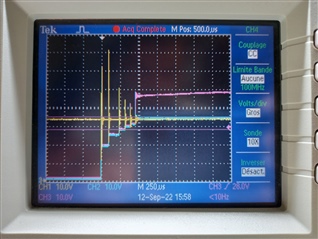
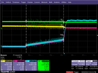
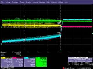
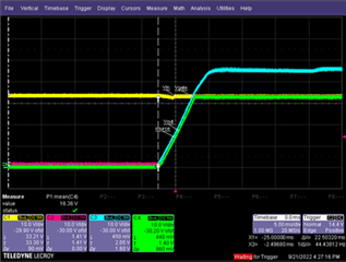
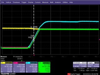
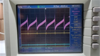
20220906_172210.jpg with Yellow = VIn, Blue = VOut, Purple = VGate

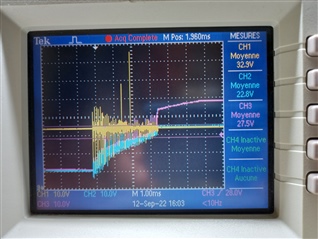
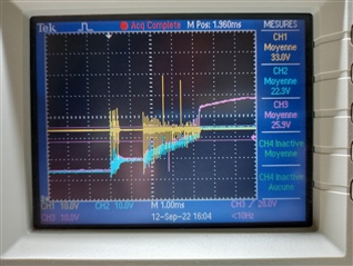
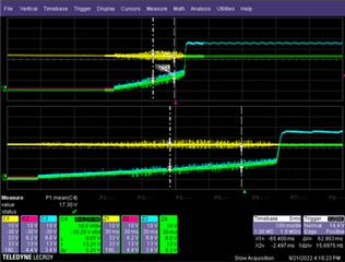
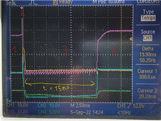
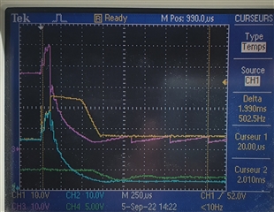
MicrosoftTeams-image (8).png, MicrosoftTeams-image (9).png, is the same test as image (8) but with a focus on the state 1 to 3.

Yellow = VIn, Blue = VOut, Purple = VGate, Green = 5V power supply on the board

 1 = initial state

2= pulse 2b activation of the OV protection

3= undefined state with a Vout around 4V and Vgate at a strange voltage

4= product come back to initial state, may be because Vin go just under the threshold, but recovery time is very long.

Could you help us to understand the phenomenon to:

  • Be sure we identify the good Root cause
  • Suggested corrective action is the good one
  • Suggested corrective action is well define

Regards,

Viktor

  • Hi Viktor,

    Let me look into this issue and get back with my comments by tomorrow.

  • Hi Viktor,

    Please see my comments below,

    1. The behavior customer is observing is certainly not an expected behavior of LM74502-Q1.
    2. While customer is testing on EVM, I assume the jumper setting of J4 is 1-2. Please confirm.
    3. Has customer tried replacing the IC with a new IC on EVM and check if the behavior is repeatable ? This is to ensure that the IC on the board is not already damaged.
    4. Is Enable signal Driven by an external Supply ? Is it stable ? Can you share waveform of the EN signal during OV test ?
    5. Have you checked VCAP pin voltage ? The voltage across VCAP-VVS must be > V(VCAP UVLO) rising threshold. Please share VCAP-VVS voltage during OV test as well. Did customer change the charge pump capacitor on EVM ? If yes, what is the value it is changed to ?
    6. What is the nature of load applied at the output ? Is the behavior same with and without load ?
  • Hi Parveen and Viktor,

    I'm the customer, please find here after my answer to your questions :

    2 J4 is 1-2 to manage OV from the input

    3 We reproduce the same shematic on the 2 location of the demo board. The second location is used as reference because component have been change and we see the same behavior.

    4 Enable signal is stable at 2.16V, we have the same behavior when enable signal is connected to VIN. EN signal and OV signals have some distrurbance when we are in the fault state but the distrurbance is synchronise with the Vgate commutation. I will send you the plot.

    At Startup

    During issue

    Yellow = VIn, Blue = VOut, Purple = OV, Green = EN

    5 Vcap-Vs is good. We try to increase the charge pump capacitor but don't see a real improvement.

    Yellow = VIn, Blue = VOut, Purple = VGate, Green = VCap

    Vcap - Vs = 40.6 - 29 = 11.6V

    6 Without load the issue disapear, we have filtering capacitor and a DC/DC as load

    Other information:

    - the defect could disappear at hot temperature and come back at cold temperature.

    - MOSfet implemented is SiR120DP

    Regards,

    Stephane

  • Hi Praveen,

    I investigate all the day to try identify some root cause. I start to understand some points but all is not clear.

    1) I do a test in overvoltage protection only by removing one MOS.

    ==> we have an improvement but defect always appear but mainly at cold temperature. Moreover the regulation voltage on Vout is between 10V and 20V instead of 4V.

    2) I do a test by replacing LM74502 component with H version but with a Rgate of 4 Ohms.

    ==> functionnality is really improved but we have always some long start but it start after a noisy time slot. Issue appear always at cold temperature.

    3) I do a measurement of our DC/DC during an issue, we see vout at a high  level to start our product but it seems not ready to deliver all the current to the load even if we have a soft start.

    Yellow = VIn, Blue = VOut, Purple = VGate, Green = 6V DC/DC output

    Issue is located between the Charge Pump capacity, Mosfet, load consumption and temperature. I dont understand why the voltage can't be available in 50ms on the output ?

    Waiting your feedback.

    For information when part is OK curve :

    Yellow = VIn, Blue = VOut, Purple = VGate, Green = 6V DC/DC output

    Best regards,

  • Hi Stephane,

    Thanks for sharing the additional information. Let me review and get back to you by end of today.

  • Hi Stephane,

    As per the waveforms shared by you, When the issue occurs (Vin less than OV threshold but Gate oscillates and is unable to ramp up),

    • The voltage on EN/UVLO is stable and is > V(EN_UVLOR)
    • The Charge pump voltage (V(VCAP) – V(VS))  is > V(VCAP UVLO)
    • The  voltage on OV pin is stable and is < V(OVF)
    • The voltage on VS pin is > V(VS_POR)

    Considering all the above points, I don't see a reason why the GATE of LM74502-Q1 should not come up.

    The most possible reason could be the FET being damaged and its gate pin is sinking current into it. This is the reason why you see an improvement when you remove one FET out of the 2 back-to-back FETs. Can you try replacing the FETs with another make and check if this issue occurs again ?

  • Hi Praveen,

    We obtain the same conclusion and I already change MOSFET. To be sur at 200% I just change MOSFET with SIR186LDP-T1-RE3 that are very close to the reference define on the eval board.

    I use LM74502H-Q1 component.

    1) Test on Eval board alone with J3 connected and C3 removed.

    Yellow = VIn, Blue = VOut, Purple = VGate

    I don't understand why there is step up on VGS and VS and why commutation time is around 500 µs ?

    2) Test on eval board connected to our application board

    Yellow = VIn, Blue = VOut, Purple = VGate

    We see the same response but with a commutation time of 3.5ms. On this picture load are capacitors and a DC/DC.

    3) Test putting   DC/DC disable to avoid consumption at recovery

    Yellow = VIn, Blue = VOut, Purple = VGate

    We see the same response but with a commutation time of 4.5ms. On this picture load are only capacitors.

    Why we have a step at 20V during 1 ms ?

    4) Try to connect eval board directly to power supply like test 1 but with our application board connected in output.

    Input TVS protection diode are disconnected.

    For the first time I have a good edge of commutation, but unfortunately the component LM74502H is broken.

    OV protection never appear because OV pin = Vin pin = 25V !!!. We alreday see this failure 3 times with LM74502H components.

    Yellow = VIn, Blue = VOut, Purple = VGate

    Something doesn't work but I really don't understand what ?

    And I have more and more pressure to found a solution.

    Best regards,

    Stéphane

  • Hi Stephane,

    In the waveforms shared, the input voltage seems to be greater than the Abs Max rating of the LM74502-Q1 IC and the FET VDS rating. This voltage spike on Vin can damage the LM74502-Q1 and the FETs. So, i would recommend you to do the following,

    1. Take a fresh EVM (to make sure the LM74502-Q1 and the FETs are not damaged ones)
      1. The default FETs on the EVM may be 30V rated. So, change them to 60V or 80V rated FETs
    2. Make sure the TVS at the input is populated (to ensure the IC and FETs are not damaged due to transients at the input)
    3. Start testing with a simple power supply and resistive load at output.
      1. Test start up and OV functionality (Make sure that the OCV threshold is less than the TVS breakdown Threshold)
    4. If the above step is passed, then start testing with your actual load/ system setup

    Going step by step as above will help us isolate the issue. 

  • Dear Praveen,

     We perform additional measurements with the new LM74502Q1 EVM.

     We do measurement Step by step with limited changes and we identified  the root cause.

     The setup is the following:

    • Use of the PSIL199 / LM74502Q1 EVM without changes
    • No output loads (except EVM LEDs and capacitors)
    • Supply definition:
      • 32.8V supply (for normal use)
      • 32.8V + 6.5V = 39.3V  (level for output voltage protection activation)

     We test the folowing setup on the new eval board and demonstrate our issue is directly linked to the MOSFET internal caracteristics,

    • DMNH6012SPSQ MOSFET which are the reference mounted in the EVM.
    • SIR120DP MOSFET instead of Q3 and Q4
    • SIR186LDP MOSFET  instead of Q3 and Q4
    • EVM back in initial condition with our UDA load.

    LM74502Q1 EVM measurement without changes (MOS reference: DMNH6012SPSQ)

     DMNH6012 recovery after overvoltage (LM74502Q1EVM_DMNH_Recovery.png)


    LM74502Q1 EVM measurement with changes (MOS reference: SIR120DP)

     SIR120DP recovery after overvoltage (LM74502Q1EVM_SIR120DP_Recovery.png & png )


    • Conclusion: There is an  issue at LM74502 with the SIR12DP MOSFET but during the recovery (after an overvoltage). The LM74502Q1 with these MOS is not as quick as the EVM design (same behavior as we had in our first eval design). It takes 80ms to have a recovery to normal condition. Unstability on the gate.

     LM74502Q1 EVM measurement with changes (MOS reference: SIR186LDP)

    • SIR186LDP recovery after overvoltage (LM74502Q1EVM_SIR186LDP_Recovery.png )
    • Conclusion: Same behavior with the SIR120DP, but the recovery time is around 182ms

    The main differences on the MOS datasheet are located on parasitic capacitor, and we investigate on the Miller effect after TI and internal recommendation.

    We identified that the Crss (gate source capacitor) is different:

    So we test with a 100pF capacitor between Drain and gate of the first Mosfet and we solve our issue.

    How we solve the issue ? :

    So we test with a 100pF capacitor between Drain and gate of the first Mosfet and we solve our issue.

    Without Drain Gate capacitor                                                             With Darin Gate Capacitor

    We also test with only a Rgate of 100 Ohms on each MOSFET, as close as possible to the MOSFET Pin

    Issue Understanding :

    Analysis from TI : Upon more research  I could find a clear explanation for this behavior in a Application note from Toshiba.   In summary, the root cause is that there will be oscillations between gates of parallel FETs (especially with high gm) due to FET and circuit patristics. In our circuit, the back-to-back Mosfets can be considered as parallel Mosfets in small signal analysis. This issue occurs when multiple FETs are in parallel and this is the reason why you see the issue only when back-to-back are connected and do not see it when only one FET is present in the circuit.  As you figured out, one solution to resolve the issue is by adding additional capacitance across FET Gate-Drain.

    For more understanding on this issue and possible other solutions, please refer to the above application note sections ‘3.2. Parasitic oscillation of parallel MOSFETs’   and ‘3.3. Supplemental explanation’. You can also see simulation results in section’4.2. Parasitic oscillation between parallel MOSFETs’.

    On our side, we investigate to avoid oscillation on gate MOSFET, the capacitor between drain and gate is not the right solution for EMC so we work on gate resistor.

    Conclusion :

    Issue is association of High power mosfet at high voltage with a bad gate layout on the eval board. This association generate an oscillation initiated by the Miller Effect. The schematics is equivalent to MOS in parallel, and is well documented.

    We add a 100 Ohms gate resistor on each MOS and as close as we can of the Gate pin of the MOS and all is OK whatever the temperature, the MOS and the load .

    How to justify and demonstrate by calculation that Rgate value is the good one to avoid oscillation ? We are searching the answer,

  • Hi Stephane,

    Thanks for summarizing the issue and solution.   As you can see from the Application note, the cause of oscillations is the parasitics of the FET along with the path inductances which for a Colpitts oscillator. The resistances in series with gate of each Mosfet will help dampen the oscillations. We have seen customers using the gate resistance value generally in the range of 2Ω -10Ω. The app note also demonstrates the results with gate resistances of 2Ω. Higher the resistance value higher the damping of the oscillations. So, the value of  100Ω should be good enough. Calculating this value may be difficult as it requires estimation of all parasitic components.