This thread has been locked.

If you have a related question, please click the "Ask a related question" button in the top right corner. The newly created question will be automatically linked to this question.

TPS386000: CTn Voltage Delayed on Single Channel

Part Number: TPS386000

Our design has 5 voltage rails that are connected to the SENSEx inputs on two TPS38600 devices - V1 (SENSE1-1), V2 (SENSE1-2), V3 (SENSE1-3) and V4 (SENSE1-4) on device 1 and V5 (SENSE2-1) on device 2. Note that VDD of both devices is V4. These rails are connected to the SENSEx inputs through voltage dividers that equate to approximately 0.410 volts when each rail is in regulation. This 0.410V exceeds the SENSEx threshold (VIT- of 0.4V +/- 4mV) which causes the devices to kick off the delay timer. Once the delay timer has expired, the device releases the POR output and the signal goes HIGH via a pull-up resistor. We’ve programmed the timer to be 90.5 ms per the equation in the datasheet which equates to a CTn capacitance of 0.022 uF (22 nF) for each input.

Our understanding is that there are two conditions required for the 90.5 ms programmable timer to start.  In addition to the SENSEx input exceeding VIT-, VDD also needs to exceed 0.9V.  All 5 *RESET outputs are wire OR’d together so the POR is not released until the last timer has expired.

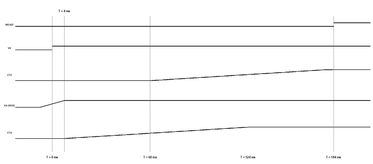
There are two issues we've encountered. 1. Every rail's CTn input starts to ramp up almost immediately when VIT- > 0.4V and VDD > 0.9V except for V2 which is way off and looks to be started about 60 ms later than expected.  Also, all of the CTn ramps from 0V to 1.24V are approximately 120 ms and not 90 ms as I would expect based on the capacitance value chosen. I thought maybe the parasitic capacitance on the board would be contributing but we measured using an LCR meter and it was in the pF range. If we make several assumptions such as the capacitance being on the high side (1% tolerance), the CTn current being on the low side (235 nA), and the CTn threshold being on the high side (1.299V) then the actual hardware just barely meets the calculations in the datasheet. However it seems unlikely the device would be operating at the limits in all the aforementioned parameters. Any thoughts?

  • Hi Shane,

    I just have a few questions:

    1. I understand that the ramp time of the capacitor voltage is 120ms, but is the Reset de-assertion delay also 120ms?
    2. For the V2 behavior, is the Sense2 and Reset2 also exhibiting the 60ms delay?

    Jesse 

  • Hey Jesse,

    please see responses below:

    1. I understand that the ramp time of the capacitor voltage is 120ms, but is the Reset de-assertion delay also 120ms?
      1. When you say "Reset de-assertion delay" I assume you're referring to the delay time between when both the VIT- threshold is crossed and VDD reaches > 0.9V, and the device releases *RESET. This delay is 176 ms and is measured from when the last rail - V4 (VDD) which is lagging V2 by only 4 ms - reaches regulation to when the wire OR'd reset is released (and pulled high via a pull-up resistor). Despite the CTn ramp of V4 occurring almost immediately after V4 reaches regulation, the 60 ms delay of V2 is delaying the release of *RESET. The 180 ms is a result of the 4 ms time differential between V2 and V4 reaching regulation, the 60 ms delay on starting the CT2 ramp and the 120 ms CT2 ramp itself ((60ms - 4 ms) + 120 ms).
    2. For the V2 behavior, is the Sense2 and Reset2 also exhibiting the 60ms delay?
      1. Reset2 is wire OR'd with the other RESETn outputs. The releasing of the wire OR'd output coincides with CT2 reaching 1.24V then discharging. The other CTn ramps discharge before the wire OR'd output is released. Channel 2 is the only channel that is experiencing a 60 ms delay between the rail reaching regulation and the CTn starting to ramp. All other ramps start immediately or have a 3 or 4 ms delay.
  • Hi Shane, 

    Are you able to provide a probe image for CT2, Sense2, RESET2 and VDD during ramp up?

    Yes the time between Sense pin goes above Vth and Reset releasing is the time delay determined by the CT capacitor, given that the VDD is above .9V. 

    Also just to double check, the capacitors are directly connected to CT pin and ground.

    Jesse 

  • The capacitors are directly connected between each CTn pin and ground. The ground is common.

    Below is a mock up of what we're seeing. As you can see, CT4 ramps immediately but CT2 is delayed.

  • Hi Shane,

    Let me run some simulation and check with the design team. I will update you tomorrow.

    Jesse 

  • Hi Shane,

    So far, I am not seeing the same issue as you on my EVM. Are you able to provide the snippet of the schematic that you are using for this device?

    Jesse  

  • Am I able to reach out to you via email for further discussion?

  • Hi Shane,

    I just sent you an email.

    I will close this issue here for now as we further discuss the issue through email.

    Jesse