Hi,
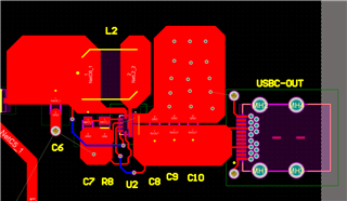
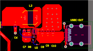
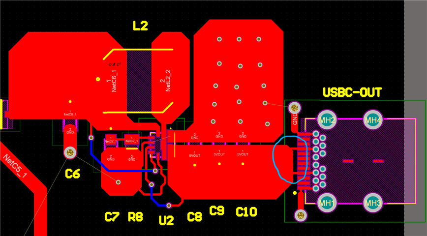
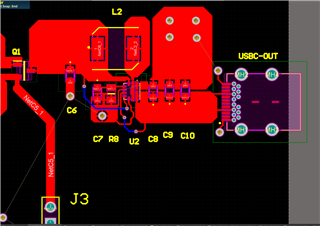
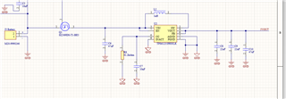
Please review my pcb layout. Ideal 5.1V/3A max output with using the CC feature to limit current to 3A. I have not created a GND polygon pour to connect all the GND connections because of difficulty to see traces and compnents for reviewing. I have a made a polygon pour for analog ground and connected a GND via to represent the single point connection between analog and power ground.
Thank you,
Andy