This thread has been locked.

If you have a related question, please click the "Ask a related question" button in the top right corner. The newly created question will be automatically linked to this question.

LM5039EVAL: Using the LM5039 in a half-bridge boost converter

Part Number: LM5039EVAL
Other Parts Discussed in Thread: LM5039, , LM5110

Hi guys,

I want to use the LM5039 in a half-bridge boost converter. I want to convert a12V input voltage that comes from a battery to a 24V output voltage. I'd like to use the LM5039 and the LM5039EVAL board to de-risk my application. 

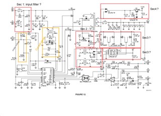
After looking at the LM5039EVAL schematic, they are a couple of circuits that I don't understand their purpose. Would you guys be able to help me with that please? They are the circuits highlighted in red in the below picture.

Also, the LM5039EVAL converts a [36V-75V] input voltage to a 3.3V output voltage. Would there be any ways for me to modify this board so that it converts a 12V input to a 24V output? If not, are they any other eval boards available that I could use to test my application?

Sections I can't seem to understand : 

  • Sec 1 
  • Sec 2 
  • Sec 3
  • Sec 4

Thanks a lot for your time.

  • Hi Amine

    My support team experienced some E2E coverage reassignments this week that involved a slight mix-up so my apologies for the delay here. Please allow me to start by explaining what each of the blocks are in the schematic you posted:

    1. Section 1: C38 is a Y-capacitor used to help mitigate common mode noise. This is often necessary for passing EMI standards such as CISPR 32, CISPR 25, etc. The location of this capacitor is usually placed directly across the isolation barrier (transformer) and must be rated to handle the full isolation voltage (2kV in this case). L1, C3-6, R1, R3, R4 form an input filter. The push-pull is a buck derived topology and like all buck topologies (isolated or non-isolated) it sees a pulsing AC input current. Adding the input filter make is appear more like a current fed buck where L1 is a "current source" - this again is better for EMI performance, if that's important to you.
    2. Section 2: A simple series pass regulator (like an LDO) used as a post regulator to the T1(1-5) winding to regulate the VCC bias supply voltage to the LM5039.
    3. Section 3: This is the first "section 3" and this is your output rectifier which uses MSOFETs instead of diodes. Here you have 2 parallel synchronous rectifiers (SRs) in each positive and negative switching cycle. The parallel pairs have common gates driven asynchronously by a gate driver IC (LM5110). Using SRs on the output stage is an indication that this is a high output current design.
    4. Section 3: This second "section 3" has T3, T4 as gate drive transformers used to pass the SR gate drive signal from the primary side to the secondary side. Notice that each of these gate drive transformer outputs are seen as inputs tot eh LM5110 SR gate driver IC.
    5. Section 4: This is a diode rectifier followed by a series pass regulator. Since this output is using diodes as opposed to SRs, it is most likely low current and it is not fed back to the controller so the regulation is poor and this is why a post regulator (series pass regulator) is required.

    One helpful tool for deciding on a power topology is TI Power Stage Designer which you should download and try. You can pick a topology, enter your design requirements and you will know what modifications must be made to the power stage. You can also search the TI Reference Design Database and see if there are any designs close to your requirements. Thanks for connecting through E2E and again, I apologize for the delay.

    Regards,

    Steve M