This thread has been locked.

If you have a related question, please click the "Ask a related question" button in the top right corner. The newly created question will be automatically linked to this question.

UCC27517: Noise applied to IN+ pin

Part Number: UCC27517

Hello,

I would like to ask you about the UCC27517DBVT device.
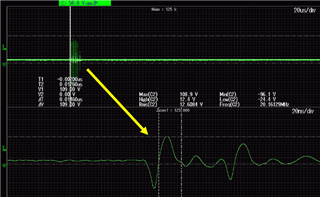
We are checking the short circuit between IN+(3pin) and GND(2pin) of this device.
(Question)
Will the device destroy if the attached waveform is applied between IN+ and GND?
Since the device has a resistance of HBM4kV, if the noise applied in the attached waveform is the cause of the device breakdown, is it more likely that it is insulation breakdown rather than thermal breakdown?
The waveform has a rise time of several nanoseconds, and the width of one pulse is as short as just under 20ns, so I don't think the amount of heat applied is as high as HBM4kV.

Best regards,

  • Hello Kaji-san,

    I agree that the heat isn't that high due to the short duration. It is a violation of the input's absmax specs, but only for a brief amount of time. It is usually very difficult to determine the balance of time and voltage that will break the input ESD structure. I did find a thread about latchup testing that could be slightly relevant, but I'm not sure. I've attached it here just in case. 

    So to summarize, I do believe such a waveform could damage the device. I think our latchup specs could be exceeded and cause an event that shorts the pins. The 'A' version of this device has more robust input pins, but since this is more of an esd-type event it may not help much in that respect. I would actually suspect the undershoot pulse as being the more likely culprit for breaking this device, based on the ESD structure and datasheet ratings. I believe HBM has no voltage undershoot, so it may make more sense to compare to CDM. 

    Thanks,

    Alex M.