This thread has been locked.

If you have a related question, please click the "Ask a related question" button in the top right corner. The newly created question will be automatically linked to this question.

UCC27538: UCC27538DBVT QUESTION

Part Number: UCC27538

Hi Team,

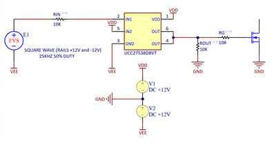
I have an application that uses UCC27538DBVT as a MOSFET gate driver, and I'm experiencing a weird problem. The UCC27538DBVT IC is getting hot without a reasonable explanation, according to a simplified schematic below.

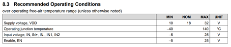
According to the device datasheet the recommended operating conditions are:

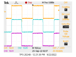
My application uses 24V power supply (+12V and -12V) to power the device and for the pin 5 (IN2).

The input signal is 25kHz, 50% duty square wave.

Problem:

When I connect the input signal directly to pin 2 (NO RIN), the device starts to get hot. If I leave it on for a while, it will most likely damage the device. (it reached 80C when I turned off the power to avoid damage to the device).
As a workaround, I added a 10K resistor (RIN) in series with the input signal, and it works fine.

Any idea why the device is getting hot without RIN?

Thanks for considering my request.

Carlos

  • Hello Carlos,

    My guess is that there is something with the input pin's esd/input structure that is causing it to source/sink more current than expected. This would heat up the device, and placing a resistor to limit the current could fix it like you are seeing. Can you attach a capture of IN1 with respect to VEE to help me understand the exact voltage levels? Also, when you attach Rin for this test are you still switching the output? Lastly, what is the gate capacitance of the load you are driving? 

    Thanks,

    Alex M.

  • Hi Alex,

    Thank you for the prompt reply.

    Answering your questions:

    1-When there is no RIN, I have the same 25khz input signal, the device starts to heat up, and the output voltage is always high (+12V). When the RIN is connected, the device works fine, and the output voltage swings from +12V to -12V with respect to the ground, picture below.

    2-We are driving two INFINEON MOSFETS IAUS300N08S5N012 in parallel. The MOSFET input capacitance is 12.5nF.

    3- Please find below the requested signals.

    Channel 1 (Yellow): Device output voltage with respect to ground.

    Channel 2 (Blue): Device input IN1 with respect to VEE.

    Channel 3 (pink): Signal Generator with respect to VEE. There is about 1V drop across RIN.

    PS. The scope has isolated channels. 

    Thanks

    Carlos

  • Hi Carlos,

    Thanks for the scope captures; it helps a lot. For this device, there is a pulldown on IN1 of about 230k. Adding the series 10k essentially makes a voltage divider. Using V = 24* (230/10+230), I get exactly 23V on IN1 due to the voltage divider, which I believe explains your drop and rules out any unexpected current. 

    When there is no RIN, how does IN1 look? The reason I ask, is that if your square wave generator cannot sink current on the negative phase, the pin could float and that would explain the output staying high. Otherwise, my only other idea would be that your signal was tripping the ESD protection. 

    In any case, the datasheet does recommend adding a series resistance for inputs with amplitudes >15V, which you effectively have here. The device has TTL inputs with fixed thresholds, so it may ultimately be better for the device to give it some margin with the voltage divider. 

    As a last suggestion, removing the 10k pulldown might help also. It is referenced to ground rather than VEE, so it could fight the driver outputs in unexpected ways.

    I will mark as resolved for now as the series resistor is recommended by the datasheet (in this condition) and seems to help it work, but feel free to reply with more questions/details. 

    Thanks,

    Alex M.