FAQ: How to use a dual input half-bridge driver with a single PWM signal
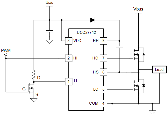
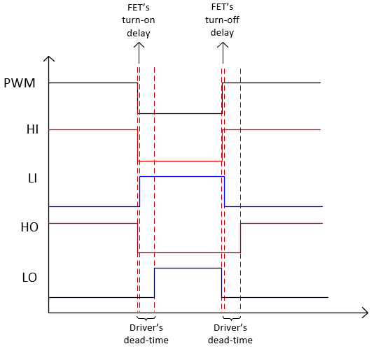
An easy way to convert a half-bridge driver with dual inputs to work with a single PWM signal is to add an inverter/not gate at one of the inputs. A simple circuit with an NMOS FET in open drain configuration and a pull-up resistor can be used. As shown in the schematic, the gate of the FET is connected to the PWM signal, the source is connected to GND, and the drain is connected to the driver’s LI pin and pulled up to VDD through a pull-up resistor. The time vs. voltage plot shows the behavior of the circuit. When the PWM signal is HIGH, the FET will be closed and LI will be pulled down to GND, and when the PWM signal is LOW, the FET will open and LI will be pulled-up to VDD. This results in complimentary HO and LO outputs.
A key consideration with this solution is to use a driver that has an integrated dead-time feature to avoid a shoot-through event at the moment when both inputs are switching. An example of TI’s half bridge drivers that can be used with this implementation are some of our 600V drivers such as UCC27710 and UCC27712/UCC27712-Q1 with 150ns typical dead-time. If a driver for lower voltage applications is needed, the following drivers operate with a single PWM input: LM5106, LM5105, LM5104, LMG1210, TPS28225-Q1.


Note: For information about implementing a single PWM when using a half-bridge driver with dual inputs and without an integrated dead-time feature, see the solution proposed in this blog: https://e2e.ti.com/blogs_/b/powerhouse/posts/control-a-gan-half-bridge-power-stage-with-a-single-pwm-signal
If you have further questions about this topic, or any other topic, please post a new/related question and our team will be happy to help you.

