This thread has been locked.

If you have a related question, please click the "Ask a related question" button in the top right corner. The newly created question will be automatically linked to this question.

TLV702: Schematic review request

Part Number: TLV702

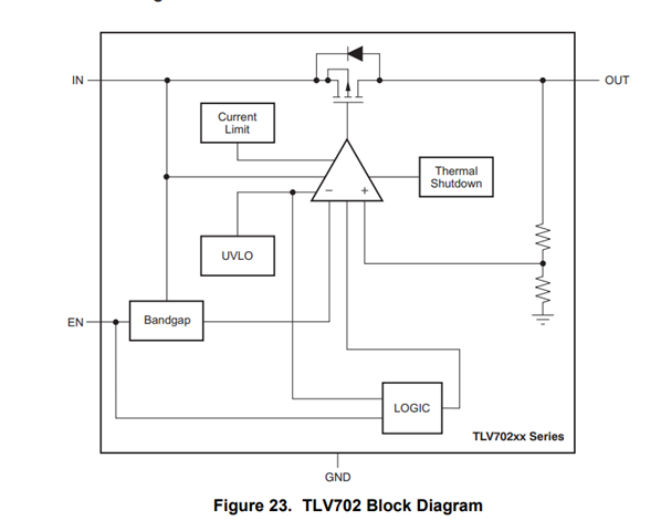
Need some help to review this circuit. The 3.3V output of TLV70233PDBVR is the power supply of the MCUs. 

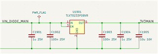
With this design we have three boards' MCU got burned. (MCU's Vdd was shorted to GND). TLV70233PDBVR seems OK after MCU got damaged(Vin was not shorted to VOUT, and VOUT was not shorted to GND). We are using this design for two different MCUs and both of them got damaged, so it might not be MCU issues.

If you have any ideas of what went wrong, please let us know. Thanks.

  • Update: I provided wrong info in my previous post. The part number in the schematic should be TLV70233DBVR. 
     Additional info.: We were using the same design for our previous Rev. and had not issues. But we used TLV70233PDBVR for the old design (TLV70233DBVR for new design). From the datasheet, TLV70233PDBVR has output discharge circuit, but in our design EN signal is connected to VIN, how does this discharge circuit effect the output? or the performance of the regulator?
    Thanks!

  • Hi Ke,

    The design seems fine, however it may be necessary get some data on the signals of the system.

    The active output discharge version of this device (P-version) has an internal pulldown MOSFET which connects a resistor from OUT to ground when the device is disabled to actively discharge the output capacitance. The active discharge circuit is activated by driving EN low or by the voltage on IN falling below the undervoltage lockout (UVLO) threshold. 

    The discharge circuit should be inactive as long as EN is driven high and VIN is within recommended operation range. 

    Below is a comparison of how the non-P and P-version of TLV702 differ internally.

    I would like to know more about your system:

    Are the MCU's damaged the moment the LDO is switched on or once it has been switched off?

    Do you have some data on the input and output signals of your system at different times? (Such as start-up and shut-down)

  • Hi Andres, 

    Thanks a lot for your quick response. We have no idea of when the chip got damaged (power on or power off) because the board worked from beginning and failed later. Originally I thought the regulator was the only issue but after removing the regulator 3.3V still shorted to GND, then I realized that the MCU might get burned. After replacing the MCU and the regulator, the board was back to work. I will probe 3.3V output when I power on and off the board and upload the waveforms here.