This thread has been locked.

If you have a related question, please click the "Ask a related question" button in the top right corner. The newly created question will be automatically linked to this question.

TPS7A16A-Q1: Restrictions for rise/delay time

Genius 13919 points
Part Number: TPS7A16A-Q1

Hi Experts,

Good day.

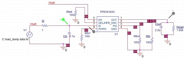
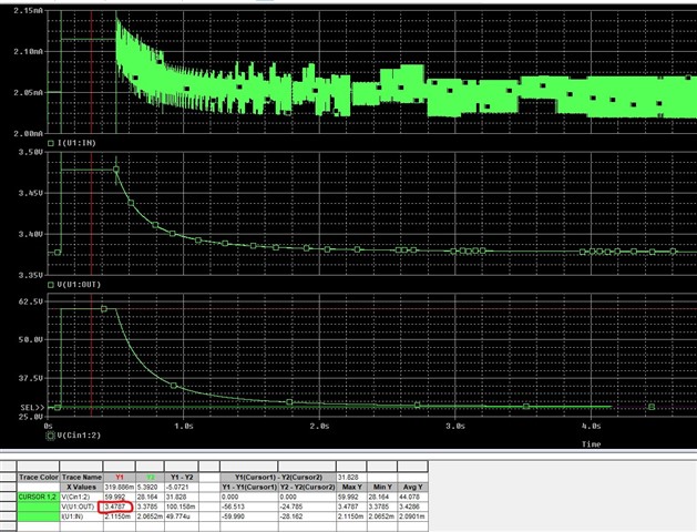
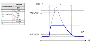
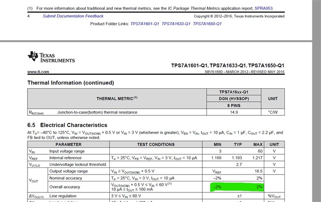
We knew that readings outside specified from absolute rating from D/S of TPS7A16A-Q1 would damage it. But we would like to know if there are some restrictions to comply in terms of rise and delay times in case of a load dump pulse transient is applied to the Vin input pin for the device TPS7A16A-Q1:

For your confirmation.

Thank you.

Regards,
Archie A.

  • Hi Archie,

    I'm looking into this. I'll get back to you in 1-2 business days. 

    Regards,

    Nick

  • Hi Archie,

    Our devices are simulated and tested with 2V/us slew rates at the pins. Anything faster than that is kind of unknown territory, but I've done testing with faster slew rates than that with no issue; we just don't have a good way to give you confidence with faster slew rates. 

    Regards,

    Nick

  • Hello Nick,

    Thanks for clarifying about the slew rate.

    I wonder if TI have a model for the load dump description that our customer can use in our tool.

    Regards,
    Archie A.

  • Hi Archie,

    Not that I'm aware of. I can try running some transistor-level sims to see if I notice any weird behavior, but I don't know if I'll be able to replicate the full load dump waveform. I think what's important anyways is the slew rate seen at the input (assuming no abs max violations), so if they can estimate the maximum dV/dt then I can try.

    Regards,

    Nick

  • Hello Nick,

    Thanks for the info. Cx responded:

    We are simulating using PSPICE and the model provided by TI (sbvm111.zip), also simulating a load dump transient, attached is the simulation circuit for device TPS7A1633-Q1 (3.3V fixed, according datasheet), I had to add Rfix resistors to avoid simulating error because PSPICE is expecting to have pins 2,3,6 and 8 not floating.
    Required output current is 2mA (1.65Kohms).

    But when load dump pulse is present, the output seems to move to 3.4787V (V(U1:OUT), cursor Y1), but I was expecting to see something in the range of 2% of tolerance according the datasheet (I am attaching a screenshot of the datasheet where tolerance is specified).

    As you can see, I am using an input capacitor of 0.1uF and and output capacitor of 2.2uF.

    Am I missing something in the circuit? or what could be the reason to have the output out of 2% of tolerance?

    Regards,
    Archie A.

    load_dump data.txt

     \

  • Hi Archie,

    The LDO PSPICE models will likely not align with EC specs. They are behavioral models and do not represent transient/stability performance well. 

    With that said, this load dump is effectively a line transient to the LDO, and the VOUT accuracy spec is a DC spec, i.e. it does not include transient performance. 

    Regards,

    Nick