This thread has been locked.

If you have a related question, please click the "Ask a related question" button in the top right corner. The newly created question will be automatically linked to this question.

BQ24616: Separate Vcc and DC-LINK rails

Part Number: BQ24616

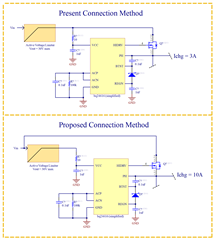
I am presently using, with success, the bq24616 to charge a 6S lithium battery at a maximum charge current of 3A. The voltage input into the system is typically 28V.  To prevent any voltage spikes on the bus from damaging the bq24616 IC, I have placed an active voltage limiter circuit in front of the bq24616 charging circuitry.  A simplified example of this is shown in the image below.  The active voltage limiter design uses a P-Channel MOSFET, so the on-resistance is on the order of 20mR.  At 3A charge current, the power dissipation in this pass MOSFET is acceptable as long as it is not actively limiting the voltage.  At a system-level, the controlling MCU stops charging if the input voltage rises above 30V.  The limiting circuitry is meant to allow the bq24616 to survive, but not charge, during input overvoltage events.

A new feature request of this design is to increase the charge current to be in the 8A - 10A range.  I am concerned about the power dissipation in the series voltage limiting circuit (the P-channel pass MOSFET) with the higher charging current, even with the voltage limit circuit not being active, the 20mR Rds of the fully-on P-channel MOSFET will still be present so I will now be rejecting  single-digit watts of heat.  See the "proposed connection method" shown in the bottom half of the image below.  In this proposed schematic, the active voltage limiter circuit only has to supply the operation current of the bq24616 itself, with the primary battery charge current being drawn directly from the input voltage bus (what I refer to as DC-LINK in the title, referencing terminology used in SVPWM aka BLDC motor controllers).  I do not expect Vin to exceed 30V for anything more than a moment, but with this topology, it seems that I could continue to charge at 10A well into the 30s and 40s of volts, should that ever occur (again, it won't).

This is a design update and I am looking to minimize copper changes, to reduce project risk as much as possible.  I also understand that changing the power feed of the bq24616 may introduce its own risk.  My question to the TI experts is whether they see any specific caveats or drawbacks to this proposed design.

Thanks in advance for any insights or suggestions,

Will

  • Hi Will,

    BQ24616 can support 10A charging itself. I will ask my colleagues for more input on your proposed connection. Right now the concern I am seeing here is that where will the input sense resistor be placed, what are the OVP for pins connected DC-Link (if there are any), and the rating of the FETs connected to DC-Link.

    Regards.

  • I do not use the input sense resistor.  That is why I show ACP and ACN connected effectively to ground (and ACDRV is NC in my present design)

    I agree that I need to have enough margin on the MOSFETs.  Right now I have 40V parts, and may want to move up to 60V parts.
    My thought is that all the pins associated with the output stage will see no more voltage than they would normally, as those voltages are dictated by the battery voltage.  Unless I am missing a sneak path to high-voltage that I've missed.

  • Hi Will,

    Is the active voltage limiter controlled by external MCU? If so, you will lose the IINDPM and input overvoltage/undervoltage protection functionality offered by the chip.

    This is designed to charge battery only, correct? Or is there system drawing power from the input source?

    Regards.

  • Hi Tommy,

    The active voltage limiter is standalone-analog circuit.

    I am using the bq24616 for charging only.  I implemented the rest of the power stage separately, both input and output, as the battery output is designed for 100A output.  So the bq24616 is "tacked on" in that sense to the battery system, to provide charging current.  All other battery management circuits are implemented using high-current parts and designs elsewhere.

    Will

  • Hi Will,

    So the system will not draw power when charging, correct? If so, I think your new proposed design should be ok but I will get back to you after checking with my colleagues again with the information you provided.

    I will be out of office tomorrow so please expect delay in responses.

    Regards.

  • Hi Tommy,


    Correct. The system MCU only allows charging when the externally applied bus voltage is greater than the battery voltage, and charging has been commanded.  If the external bus loses its power source, the bus voltage will droop to match the battery voltage and charging will stop. LM5050 ideal-or controllers with parallel MOSFETs ensure unidirectional current flow from the battery to the external bus.

    Will

  • Hi Will,

    Thank you for the information.

    I will get back to you when I get back.

    Regards.

  • Hi Will,

    The concern of you proposed design will be the response time of the input voltage limiter.

    The datasheet stated that 1ms to disable charge but I do not know how fast is the limiter's response time. If the response time is too slow you may put more than the absolute max on VCC and possibly break the part. In general we do not want more voltage than the recommended operating condition

    If the limiter response time is fast enough then I think your proposed design should be fine.

    Regards.

  • Tommy,

    Thank you for your time spent on this question, I appreciate it.


    The observation on the response-time of the input voltage limiter is a good one.  It's been a while since I did a phase margin analysis on the limiter ckt, but a quick simulation of an input step has the circuit settling out within about 5uS with about 5% overshoot.  I will be sure to keep the performance of the voltage limiter circuit in mind as I complete the charger design.

    Thanks again,

    Will