This thread has been locked.

If you have a related question, please click the "Ask a related question" button in the top right corner. The newly created question will be automatically linked to this question.

TPS40345: How to get TPS40345DRC AC model using Webench or otherwise?

Part Number: TPS40345
Other Parts Discussed in Thread: TPS40303

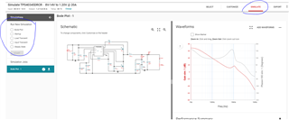
Not able to get the AC model for DCDC converter designed using TPS40345DRCR in Webench power designer tool.  When exported to TINA TI, every time only transient model gets exported. 

The website for TPS40345 only contains transient model.

  • Hello Amit, 

    Unfortunately we do not have an AC model for this device. you can use the simulation tool in the webench to run the following simulations as below  

    Thanks 

    Tahar

  • Thanks Tahar for the reply. However I wanted to customize certain components (for eg adding a parallel cap to output) to the schematic, which I suppose I can do in TINA TI but not in Webench. Please also let me know if it is possible to do the same in Webench.

    Note: I understand that I can create a custom part to suit the needs of the design. But I am not sure if the simulation results will be reliable enough.

  •  

    As Tahar points out, we don't have an average (AC) model for the TPS40345.  I also checked the TPS40303/4/5 devices, which use the same voltage mode control modulator, and unfortunately we don't have AC average models for them either.

    Since the TPS40345 uses voltage mode control with a VDD/6 ramp amplitude, you can approximate the AC performance with a couple of amplifiers, if you don't need to model start-up or current limit.

    First, model the Error Amplifier with a 25MHz Gain-Bandwidth Product Operational Amplifier with a 80dB (10,000) DC gain and 2.5kHz single-pole roll off.  The output impedance up to the 2mA current limit is about 200Ω.  Connect the 600mV reference to it's non-inverting pin.  FB is the inverting pin and COMP the output.

    Second, model the Modulator and MOSFETs as a voltage controlled voltage source with a forward gain of 6 clamped at VIN and GND and an output impedance equal to the Rdson(HS) * (Vout/Vin) + Rdson(LS) * (1-Vout-Vin).  The Error Amplifier's output (COMP) voltage will drive this voltage controlled voltage source.  Add a 1V voltage source to the negative input of the Voltage Controlled Voltage Source to represent the valley of the modulator ramp.

    If you want to add the AC response of the switching, divide the output impedance above by 4, then use 2 resistors of that value to build 2 RC filters at 1.4x the switching frequency and 2x that value (1/2 the calculated output impedance) between the second filter capacitor and the switching node.

    That should be good enough for most applications upto 1/3 of the switching frequency (200kHz)