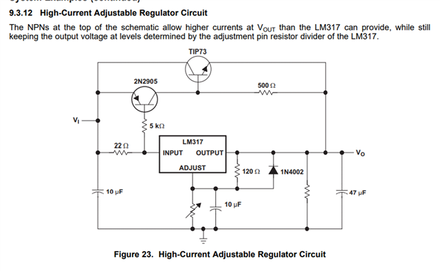
Do we have any design guide for below circuit with LM317 solution?
Customer want to know the power loss of LM317 and TIP73 and to see whether below circuit is suitable for the demand voltage and current or not?
Input Voltage:20V
Output Voltage:15V
Output Current:700mA Continue,1A Max.