This thread has been locked.

If you have a related question, please click the "Ask a related question" button in the top right corner. The newly created question will be automatically linked to this question.

TPS62912: Undervoltage transient at the top of the ramp

Part Number: TPS62912
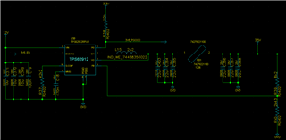
Other Parts Discussed in Thread: , TPS62913

Hello,

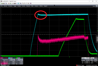
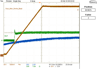
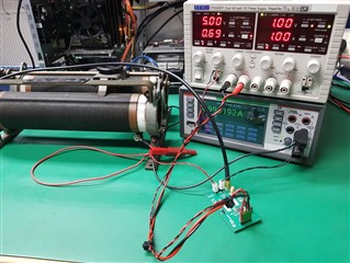
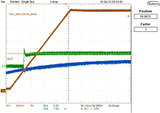
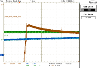
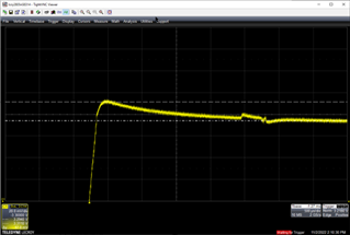
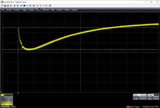
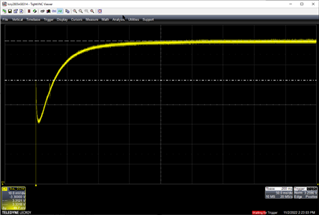
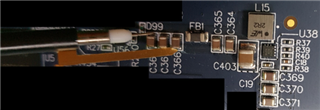
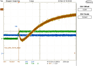
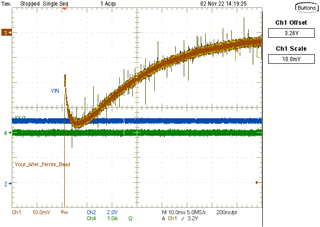
I'm using a TPS62912 in my design, and notice that there is a large undervoltage transient at the end of the soft-start sequence on all four instances of this power supply on my board.  This transient is also on the evaluation board fresh out of the box with default components and jumper positions.  I'm seeing the transient with both 2.2µH and 4.7µH inductors and with switching speeds of 2.2 MHz and 1 MHz.

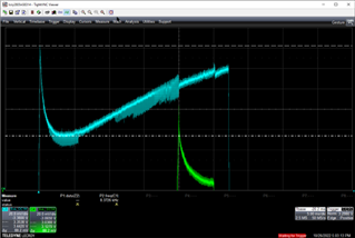
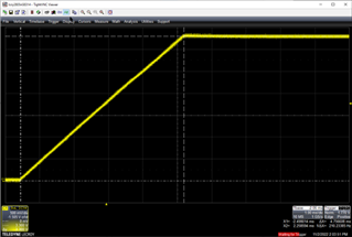
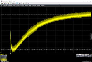
Here is a screenshot of the evaluation board output with no load fitted:

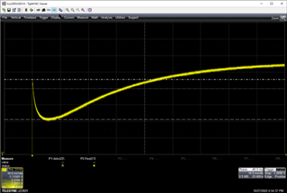
The evaluation board is generating 3.3 Volts from a 5 Volt input.

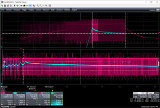
I fitted a 3.3 Ohm resistor to give a 1 Amp load, and the transient (indicated between the white cursors) increased very slightly from 24mV to 26 mV.

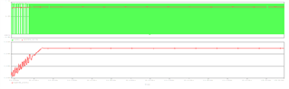
I tried input voltages from 12 Volts to 4.5 Volts in steps of 2 volts, and the input voltage made no difference to this transient.

Please could I get some support on the cause of this transient and any advice on how to eliminate, or at least minimise it?  I believe that working on the evaluation board would be a good starting point as the schematics and layout are publically available.  I would also like to solve this issue on my board, but would prefer that the details of my design might be discussed in private.

Many thanks in advance!

  • Thanks for your question. From your scope plot, I am not sure when you are seeing this behavior.  Is it at the transition from start-up to power good? Can you provide a scope shot that shows where this is happeining?

    One thing to note is that if you change the output voltage on the EVM, the effective capacitance of the output caps are reduced due to the DC bias derating of the caps. If you would like to minimize the dip during transients, increasing the output cap will help. 

  • Hi Steve,
    Thanks for getting back to me on this.

    This transient is at the end of the soft-start.  Here is a screenshot of the same behaviour on our board which shows the full soft-start behaviour:

    Here's some detail of the device switching from pulse-skipping mode for continuous PWM at the top of the soft-start ramp

    The blue trace is the filtered output downstream of the ferrite bead, the pink trace is the SW pin of the TPS62912. in the above image.

    I ran a simulation in PSpice to see whether the effect could be reproduced in simulation, but it didn't show any transient at the end of soft-start:


    The TPS62912EVM-07 EVM specifies an output voltage of 3.3 Volts in its default configuration, so I would expect the default 5×22µF capacitors to be suitable for this voltage:


    Are you able to reproduce this transient on an evaluation board?

    Is this expected behaviour from the device?

    Many thanks!

    Pete

  • Hello, 

    The dip after PG is due to the transition from PFM during startup to forced PWM, as you described above, since during PWM the SW does not sink current.  This is expected behavior for this device, as you can see in the attached scope plots, where I have a ~20mV overshoot with 5VIN, 3.3VOUT, 1A load @ 2.2MHz with a 5ms startup time.  Is there an issue with this overshoot during startup? This is well under 1%.

    Startup with VIN (Blue)

    Startup with VIN zoomed in, ~18mV overshoot during startup.

  • Hi Steve,

    Thanks for your reply.

    May I ask whether your measurements were made on the TPS62912EVM-077 in its default configuration?  If so, why are you seeing an overshoot at the top of the ramp, whilst I'm seeing an undershoots on my TPS62912EVM-077 (in its default configuration) and also on all four of the TPS62912 devices on our own PCB design?

    Our measurement (shown below) on a default TPS62912EVM-077 Evaluation board gives 27 mV undershoot, i.e. it rises up quickly to almost the required voltage and then drops by several tens of mV before rising gently to the required voltage.

    TPS62912EVM-077 Evaluation board gives 27 mV undershoot.

    Our PCB design gives 90 mV undershoot, shown below:

    90 mV undershoot on our PCB design.

    Do you have any idea why there is an overshoot on your board and an "undershoot" on both the TI evaluation board and on our PCB design?

    Many thanks!
    Pete

  • Thanks for the additional information.  The measurements I took were on a TPS62913 EVM modified for a 3.3V output. I will look into the modeling of the startup to see how the end PFM and beginning of forced CCM is modeled. The startup of the TPS6291x devices allow skipping pulses to avoid min on time issues during startup, and then transitions to forced CCM for the lowest noise and ripple performance during operation. What are the differences between the EVM schematic and layout versus your board? Where is FB sensed, as well as VO? Is your startup with VIN or with EN? Any other details you can provide would be appreciated as I look into this.

  • Hi Steve,

    Thanks for confirming this.  So the biggest difference so far is that you're using the TPS62913 for your measurements, and we're using the TPS62912 for all our measurements.

    Regarding your questions, here is a schematic of one of our TPS62912 devices regulating 3.5 Volts from 12 Volts:


    The device is enabled as part of a sequence, so the 12 Volts input is stable before this device is enabled.
    Our PCB is laid out according to the instructions in the user guide.  VO is sensed upstream of the ferrite bead.  The FB resistors are located right next to the FB pin on the TPS62912, and sense the output voltage downstream of the ferrite bead.  This is the circuit that is exhibiting 90 mV of "undershoot" as shown by the blue oscilloscope trace on my previous post.

    Many thanks,
    Pete

  • Hi,

    My colleague will give you reply later!

    BRs

    Zixu

  • Thanks Zixu and Steve.

    We really do need to resolve this issue as soon as possible and appreciate any support that you can give us.

    Cheers,

    Pete

  • Hello, 

    I looked at the start-up on a TPS62912 EVM as it comes out of the box, and I see a ~10mV overshoot with a 1A load, very similar to the behavior on the modified TPS62913 EVM waveforms I sent earlier.  I am not sure why you would see the output not reach regulation voltage on the EVM, and why you are seeing a larger output voltage transient on your board.  Your schematic looks ok.  There has to be a resistance in the path somewhere that is not allowing the FB or VO sense points to properly regulate the output.  I recommend looking more closely at the output path and the FB sense path on your board.

    Also, I would like to be able to re-create the startup you see on the EVM, as I have not been able to do so.  Is there anything else in your setup other than the input supply, resistive load, and oscilloscope probes?  Where are you applying the load?  The middle two pins on the output header are sense lines, so they are not intended for placing the load there.  

  • Hi Steve,

    Thanks for your response.

    The reason we are seeing different oscilloscope traces is because you have not set up your oscilloscope voltage and timebase appropriately (i.e. 20mV/div and 10ms/div).  The behaviour of your setup and mine is actually the same, you have just missed seeing the spike and dip that I reported.

    Here is a full description of what is going on.  I would appreciate you confirming that you get the same results as me.

    Testing with the Evaluation Board

    Test Setup

    Photograph of the Test Setup using the TPS62912 Evaluation Board

    • The evaluation board is powered by the TTI bench power supply at 5 Volts.
      • The thick cables from the output connect into input header J1 on the eval board:
        • Pins 1 and 2 (Red +ve)
        • Pins 5 and 6 (Black -ve)
      • The sense output connects to J1 through dedicated sense wires:
        • Pin 3 – Red sense +ve
        • Pin 4 – Black sense -ve
      • The output header, J2, is connected to a variable resistive load (shown in the screenshot) through a Keithley digital multimeter (DMM) configured as an ammeter
        • The red resistive load wire connects to J2 pins 1 and 2
        • The black resistive load wire connects to J2 pins 5 and 6
        • Pins 3 and 4 are not connected to anything
        • The DMM is indicating a 1 Amp load current
      • The oscilloscope connects to J5 (VOUT_FILT) through a 3-foot-long SMA to BNC cable assembly
      • The oscilloscope input is configured as follows:
        • DC 1MΩ input impedance
        • 20 MHz bandwidth limit
      • The Test PCB is configured as per out-of-the-box
        • JP1 has a jumper from pin 1 to pin 2 to enable the power supply
        • JP2 has a jumper hanging off pin 1 to the side, selecting SCONF pulldown of 52.3k
        • JP3 has a jumper fitted to pull PG up to the output 3.3 Volt power supply
        • J3 is not populated with any jumper (I’m not reading in the power good signal)
        • All resistors and capacitors are as came from the factory – we’ve not modified the board in any way

    In response to your questions on my setup:

    • There is nothing else in my setup other than the input supply, the variable resistor, DMM ammeter and the oscilloscope connection to the SMA test point.
    • We are applying one wire of the load to pins 1 and 2 of J2 and the other wire of the load to pins 5 and 6 of J2
      • The Vout sense lines on J2 are not connected to anything
      • We are not loading the sense wires
    • The Vin sense lines on J1 connect directly to the sense input of the bench power supply remote sense terminals
      • We are not powering this board through the sense connections

    Comparison to your first measurement trace on the TPS62913

    Your first measurement sets the output voltage measurement to 500 mV/division and the timebase to 1ms/division.  I have repeated that setup on my oscilloscope for a direct comparison.

    Steve Schnier’s “First Measurement” screenshot of the TPS62913 evaluation board

    Pete’s equivalent “First Measurement” on the TPS62912 evaluation board

    Your measurement on the TPS62913 and my measurement on TPS62912 show the same behaviour.  The supply ramps up in 4.8 ms and reaches a steady 3.3 Volts.  I have added vertical cursors to measure the start and end voltage.  Their values are visible in the bottom left of the screenshot, at the bottom of the yellow “C1” box.  I have added horizontal cursors to measure the startup time.  Their values are visible in the bottom right of the screenshot under the timebase configuration box.

    Comparison to your second measurement trace on the TPS62913

    Your second measurement sets the output voltage measurement to 20 mV/division with an offset of 3.3 Volts and the timebase to 400 µs per division.

    Steve Schnier’s Second Measurement screenshot of the TPS62913 evaluation board

    Pete’s equivalent “Second Measurement” on the TPS62912 evaluation board

    Both of these screenshots roughly agree.  You measure an overshoot of 20 mV, whilst I see an overshoot of 10 mV.  Note that I cannot set my timebase to 400 µs/division, so have had to use 500 µs/division as the closest setting.  Both screenshots also show a very small bump approximately 1.8 ms after the initial peak has been reached.

    Extending the time of the Second Measurement

    If you look back to my very first post, the oscilloscope trace was set to 10 mV/division and the timebase set to 10ms/division – this is twenty five times the capture time of your second screenshot.

    I’ve changed the voltage scale to 10 mV/division to repeat the measurement I made in my original post:

    “Third Measurement” – zoom in on voltage (10 mV/division), zoom out in time (10 ms/division)

    The “Third Measurement” above shows an initial peak to 3.32 Volts, followed by a negative transient to 3.303 Volts.  The voltage then starts to rise again over the remaining 80 ms of the trace.

    “Fourth Measurement” – zoom in on voltage (10 mV/division), zoom really far out in time (50 ms/division)

    A “Fourth Measurement” shows that it takes approximately 150 ms from the end of the ramp-up time for the power supply to reach a steady output of 3.33 Volts.

    Our PCB Design

    Please could you check the layout of our PCB design to see whether there is anything that might be cause for concern?

    Our PCB Design Layout with top layer in green, and bottom layer in Red

    The top layer has copper planes for the input, ground and output voltages.  The output inductor, L15, is located close to SW (pin2) on the TPS62912.  The VO pin (pin 1) is connected through a very short trace to the left-hand side of L15.

    Our PCB Design Layout with top layer in green, and bottom layer in Red.  Only the outline of layer 1’s planes are shown to clearly see the tracks of the bottom layer.  The track from the downstream side of FB1 to the top of R39 (“Rtop” of the Feedback sense) is shown in purple.

    The output sense is taken from the second stage of filter capacitors and passed through a via to a trace on the bottom side of the board, highlighted in purple in the above figure.  This connects through a second via to R39 on the right-hand side of the TPS62912.

    I’m probing this power supply directly on the output capacitors using a short copper ground blade on the oscilloscope tip to give the best possible measurement.

    Photograph of our printed circuit board and oscilloscope probe

    Measurement of the circuit on our printed circuit board at 10 ms/division

    On our board, I’m probing an initial peak to 3.45 Volts.  The voltage then rapidly drops to 3.38 Volts (-70mV drop) and then slowly rises to its rated 3.50 Volts. 

    This waveform therefore shows the same behaviour as the evaluation board, but with a more pronounced dip.

    Questions

    • Please could you take the “Third Measurement” and “Fourth Measurement” on the TPS62912 evaluation board with the same oscilloscope setup that I used, and see whether you are observing the same behaviour?
      • Screenshots of your measurements would be very helpful if you could provide them, please?
    • Can you see anything wrong with our PCB layout?

    Many thanks indeed for your continued assistance with this case.

    Cheers,

    Pete

  • Hello, 

    I took measurements as you describe, and see the same behavior as you show.  I did the measurements with CC and CR on the electronic load, and see that the dip happens as the load comes up, so a transient is expected.  However, I also see the dip without the load enabled, which is likely due to the comp response to switching between PFM and CCM operation.  This handoff behavior isn't fully modeled in the SIMPLIS model. See below for confirmation of the behavior:

    I also looked at your layout, and don't see any issue with the layout, VO, and FB routing on your board. Can you describe again the system issue you are having with this behavior?

  • Hi Steve,

    Thanks for taking those measurements and posting the images - that's really helpful.  It's good to see that our tests our now agreeing with each other and that we're seeing the same dip at startup.  So I suppose that this is simply the behaviour of the chip, and nothing that is wrong with the design, component selection or layout.  Thanks also for checking over the layout, this is also helpful.

    I don't want to go into the system issues that this is causing us on a public forum, and would prefer to discuss this in private.  Would it be possible to discuss this in confidence over email, please?

    Cheers,
    Pete

  • Yes, I sent a friend request through E2E where we can communicate privately instead of on the public forum.