This thread has been locked.

If you have a related question, please click the "Ask a related question" button in the top right corner. The newly created question will be automatically linked to this question.

TPS62869: Vos pin layout

Part Number: TPS62869
Other Parts Discussed in Thread: TPSM82866A

Hi team

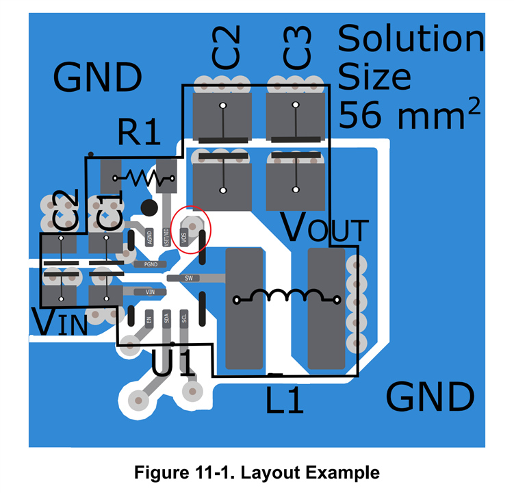
I have a questions about TPS62869 VOS pin layout:

D/S give the following layout example and here VOS pin is connected to Vout through a via, and I am wondering why VOS pin is not connected to VOUT on the top layer? 

My customer suspected VOS pin may affected by SW noise and wants to know the reason of VOS pin connection shown in the D/S. I guess this connection in the example would decrease the SW noise as possible, and if the customer connects VOS and COUT on the top layer of course this would bring large SW nose because the trace is so close to SW pin. 

May I know your comments?

  • Hi Shawn,

    I'm not sure why it is not directly connected either--the preferred connection is directly to the output cap that is right there, like you said.

    On some EVMs, we route the VOS pin in such a way that the trace can be cut in order to add a resistor to measure the bode plot.

    We also offer a power module version of this family: TPSM82866A.

    Thanks,

    Chris

  • Hi Chris

    My customer is using TPS62869 for DSP core supply and recently they found DSP is working abnormal occasionally. One suspected reason is TPS62869 output ripple. Attached please find their TPS62869  layout and I am wondering if you could help review the layout? The customer wants to know if the SW noise would affected the output ripple. 

    VOS pin and SW pin top layer layout:

    VOS connected to output through vias:

  • That should be ok.  The SW looks a little large.  Do you know where the vias on SW go? They should just connect SW directly to the inductor and not need vias to make connections on other layers.

    Chris