This thread has been locked.

If you have a related question, please click the "Ask a related question" button in the top right corner. The newly created question will be automatically linked to this question.

TPS7H4010EVM: Puzzling loop response

Part Number: TPS7H4010EVM

Hello,

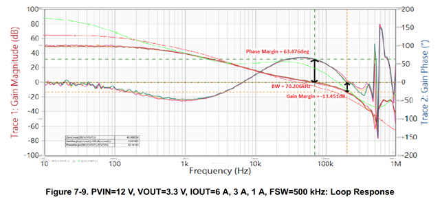
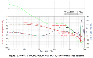
I found the loop response given in TPS7H4010EVM User's guide a bit puzzling (SNVU744 Figure 7-9 p24) : 

Considering how the phase margin is taken there is no doubt on the phase offset, so i expected the phase would be around 180° when gain slope is 0 and 90° phase when gain slope is -1 which is not the case. 

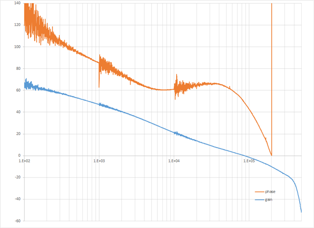
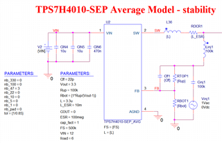
It looks like the average model of TPS7H4010-SEP is pretty much more inline with what i expect but it is not of much help if it does not match the actual converter :

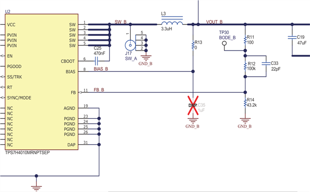
Of course i tried to match my simulation parameters (3x47uF caps are put on Vout) :

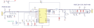
With what is actually on the eval board :

Where is the mistake ?

it should be also noted that the 1.8V side of the eval board have a loop response given in user's guide far closer to what i expect ( Figure 7-2 p20 ) :

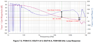
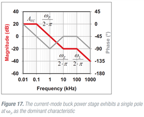
Still there is a -2 gain slope in range 1k-10kHz which to me does not match a standard current mode buck converter as for example described in slup340 Figure 17 p10 :

Thanks,

  • erf, scales error in my measure/simulation comparison, this one is better :

    Question remains the same though.

  • Hi,

    Yes, I agree the positive phase at low frequency on the 3.3V converter is interesting; since the same DUT shows the 'conventional' signature in a different configuration.  We know from transient load steps that the device is stable, however, this bode indicates it cannot be called unconditionally stable.  I plan to retest the loop response just to confirm these measurements are repeatable.  If so, I can inquire as to whether the model can be updated to more accurately reflect the device.  

    Out of curiosity, would 'conditional stability' preclude you from using this device in such a configuration?

    Thanks

    Christian

  • I generally dont like to have 0 phase margin anywhere in the bode before gain crosses 0dB. In this case I double check by drawing a nyquist plot to make sure the stability weakest point is where it should. I do not expect surprise with a buck though, but if the 3.3V loop response is the one given in user guide, there is probably something in TPS7H4010-SEP built-in corrector i do not understand, which is something we generally do not like in high reliability non-repairable products. By the way, what definition do you put on "unconditionally stable" ?

  • Yes, I agree, having phase margin past the cross over frequency is ideal.  I need to confirm the phase dip before Fco is real as I have seen significant variations in the phase measurement by changing where the ground connection to PCB is with respect to the injecting and receiving signals in the test setup. 

    My reference to unconditionally stable is meant to say that conditionally stable systems are stable only when the loop gain is within a certain range.  If this system were subjected to sufficient temporary decrease in gain, as a result of a large signal transient response for instance, the system could become unstable and oscillate.  

    I will follow up with you once I remeasure the EVM.

    Thanks

    Christian

  • Ok thank you understood. Indeed, not unconditionally stable is something we do not want, as stability justification for whole product life and any condition is at best too time consuming and at worse simply impossible. As we supply a SoC, large current transients are expected when changing mode from say standby to most power hungry algorithm/data transfert.

  • Yes, I understand the concern.  We do, however, test the device in the worst case transient load step from 0-6A to ensure stability is maintained.  I'll let you know what I find from rmeasurements.  Thanks.

  • Hello, it looks like that it has something to do with BIAS pin which is connected by default to Vout on eval board.

    When I remove R13 and short circuit C35 footprint, TPS7H4010 internal LDO automatically takes its supply at Vin and loop response is by far closer to expected curves. This would also explain difference between 3.3 and 1.8V output as LDO switches to Vin when bias pin is below 3.3V.  There is some kind of susceptibility to low frequency through this pin, so decoupling at this level is probably trickier than expected.

    I will probably post some curves from this setup soon.

  • Hi,

    Just so that you are aware, Christian will be out of the office this week due to the Thanksgiving holiday. If you can share the curves from your setup that will be useful to allow us to comment further on what you are observing. 

    Thanks,

    Sarah

  • way better with Vbias diconnected from Vout :

    curves from 3.3V side 12Vin Iout = 3A

    My setup does not allow for relevant measure below 100Hz but trend looks ok.

    SOLVED : open loop behavior is degraded when BIAS connected to Vout