This thread has been locked.

If you have a related question, please click the "Ask a related question" button in the top right corner. The newly created question will be automatically linked to this question.

LM5085: Output voltage issue.

Part Number: LM5085

Hi TI team.

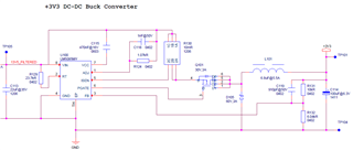
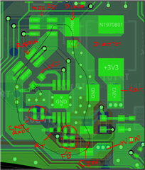
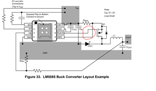
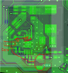
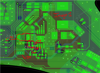
In some prototypes we designed, and we are testing, the converter is the LM5085, the output voltage should be 3.3V and maximum current are 2A. Input is 13.5V.

But we are not obtaining 3.3V, converter is not working well and that is without the load, we cannot test the converter with load because output voltage is not ok.

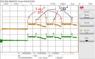
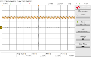
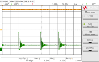
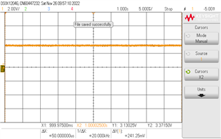
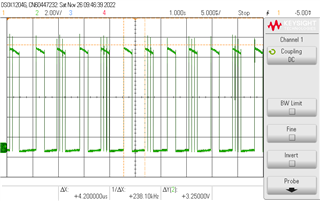
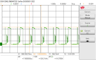
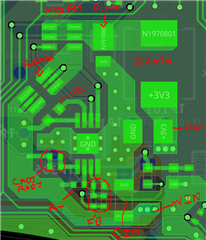
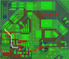
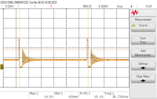
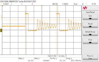
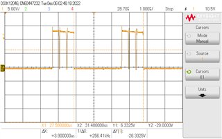
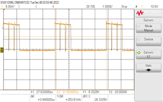
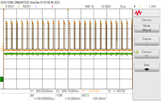
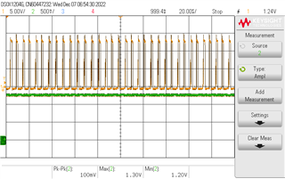
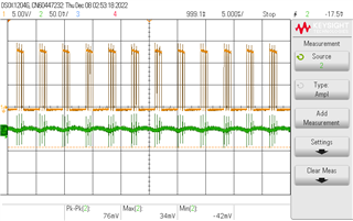
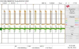
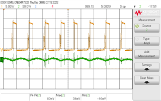
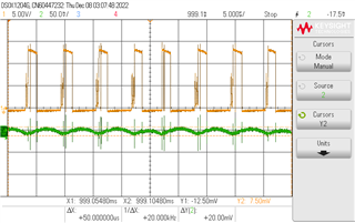
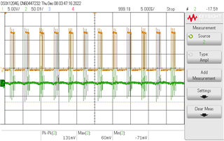
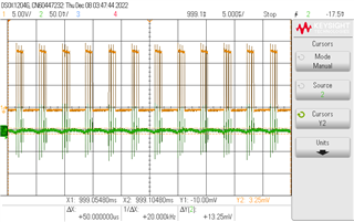
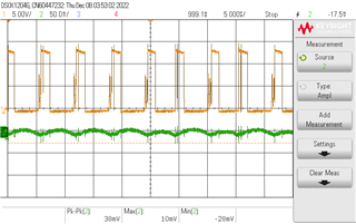
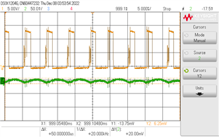
I am adding the sch and the waveform of the output voltage (yellow) and feedback voltage (green).

As you can see once we have an input voltage, the converter rises until 3.25V but immediately drops to 1.7V and when input voltage is removed, we have for 100 us 3.25V and then voltage goes low. 

So, not sure why this is happened, please check the schematic and let me know if you need more information.

  • Hi Asael, 

    Is the waveform captured with Vin=13.5V, and load=2A? And input voltage keeps supplying but you observed Vin on and off Intermittently? Please check if the current limit of the input supply is set too low to provide enough energy.

    And from the schematic, Rense and RADJ are suggested to be redesigned. 

    1. Rsense should have at least 50mV across it at maximum load current to reduce the effect of the offset tolerance of the current limit comparator. Suggest you can put value like 30mohm if current limit is set at 3A.

    2. With Rsense changed, RADJ should be changed accordingly, referring to ICL=40uA*RADJ/RSEN (Datasheet 7.3.4 Equation 9)

    I have also attached the quick calculation tool for your reference. 0045.LM(2)5085_Quick_Start.xls

  • Hi Hongjia-Wu

    About waveform captured, it is with Vin = 13.5V and current less than 50mA, we still can not test at 2A because voltage is not 3.3V.

    In fact we can not program the board because voltage is not 3.3V, so first we have to solve the converter problem to test the rest of the board

    Vin is not intermittently, sorry for the confusion, I turned on and off the input, so you can see that we can get 3.3V but only for an instant when we turn on or turn off the input, but with 13.5V always on we are seeing 1.7V.

    So, with these last comments do you think we still have to redesign the RSense and RADJ, or the cause of the problem can be different?

  • Hi Asael,

    Thanks for the clarification. Can you get stable 3.3V when there is no load at all? Do you have Vo and SW waveform when the power supply is always on? (Please mark the load condition if you share).

    Meanwhile Rsense and RADJ are still recommended to modify to reduce the offset tolerance. 

    Regards,

    Hongjia

  • Hi Hongjia.

    One comment to understand the following images. The typical input voltage is 13.5V but we designed to have from 5V to 15V as input.

    Testing above 12V (from 12V to 15V) with no load, we are having around 1.75 V. See image below (Vout-yellow line). I am not presenting the Vsw here because when I measure Vsw, something strange happens that I will address at the end of the comment

    Testing below 12 V (from 5V to 12 V) with no load we are having the right voltage, 3.3V (Vout - yellow line), as we have no load the switching frequency is low (green line), around 35 kHz.

    Testing below 12 V (from 5V to 12 V) with load we are having the right voltage (3.3V) but frequency is not correct, we should have 583.83 kHz and we are having 238.1 kHz.


    The strange thing happens when we measure Vsw with no load or load (1A) at voltages above 12V, when we place the probe to measure Vsw we have 3.3V as output (frequency is wrong, measuring 128.2 kHz), you can see the images below, but as soon as we remove the probe from Vsw, converter doesn't work again. So, not sure what is the effect of the probe in the system but with this information I think you can help us better.

    If you need more info don't hesitate to ask.

  • Hi Asael,

    Thanks for providing more details. From what you described as SW probe benefits for proper functionality, the issue could be caused by insufficient ripple at FB pin. COT need certain ripple at FB to make the control scheme work. Try a larger Cff like 4.7nF to couple more Vo ripple to FB and see if it improves.

    Hongjia

  • Thanks for the comment. We are testing that, we will test it and we will come back here with the results.

  • Hi Asael,

    Thanks for the feedback. I will close it first and if you have more findings just keep updated in the post. 

    Hongjia

  • Hi Hongjia.

    After testing, increase only the Cff doesn't help, we had to increase also the RT resistor. With a combination of 10 nF in Vcff and 90.1 kOhms in RT we can measure 3.3V at 13.5V as input without load and be able to support 0.8A with load, but with a current greater than 0.8A the converter is not working properly, presenting the same performance as commented before, so this is not functional for us. If you have comments about this, let us know.

    As we are testing prototypes and understanding problem is related with the feedback voltage, we will run a second prototype with a type 3 ripple network in feedback pin instead the type 2 to not have the issue we are having now.

    Thanks.

    Asael

  • Hi Asael,

    What are the Rsense and RADJ values when you are getting the results above? Have you modified according to previous suggestion?

    Hongjia

  • We will receive the parts today or tomorrow to adjust Rsense and RADJ, once we can run the test with those parts, we let you know but at same time working in a second design with the type 3 ripplet network in feedback.

  • OK. One more thing you can check is the ESR of the output capacitor. As you are using electrolytic capacitor, ESR should be large already. 

  • Hongjia-Wu.

    About the output capacitor we are using a tantalum capacitor with an ESR of 250 mOhms. Would you consider choosing a capacitor with more ESR?

  • Hi Asael,

    Yes 250mohm ESR should be OK.

    Hongjia

  • Hi Hongjia.

    After tested some boards changing the RSENSE and RADJ, we are having same issue. Even if we increase the Cff, we don't have changes. Only we can measure 3.3V at 13.5V as input with no load when we change RT and Cff, increasing both, and with load at 13.5V as input, only at 0.8 A maximum, with a current greater than that, converter is not working properly and that doesn't work for our application.

    Asael.

  • Hi Asael,

    What is the value of RSENSE and RADJ you changed to? And is it possible to share the layout?

    Hongjia

  • Hi Hongjia

    Rsense: 30 mOhms

    RADJ: 2.74 kOhms

    Adding the layout of the LM5085 in our board, please check it, if you need to see all the layout, I can share the gerber by email.

    Asael

  • HI

    some comments on layout:

    1. below is LM5085 layout guildline, but in your layout, the first loop mentioned below is very large.

    Two major current loops conduct currents which switch very fast, requiring the loops to be as small as possible to minimize conducted and radiated EMI. The first loop is that formed by CIN, Q1, L1, COUT, and back to CIN. The second loop is that formed by D1, L1, COUT, and back to D1. The connection from the anode of D1 to the ground end of CIN must be short and direct. CIN must be as close as possible to the VIN and GND pins, and CVCC must be as close as possible to the VIN and VCC pins.

    2. in the same time, it is better to have a input cap 0.1uF dedicated for LM5085

    As the layout reason, the FB is very near Vin trace(the Vin trace is noisy due to layout), can you try to add a 100pF at R132 see any help , but in the same time, you can also increase C119 to 10nF.

  • Hi Daniel Li14.

    Thanks for those recommendations.

    We do the following marked in the image, changing the position of CIN to reduce the first loop (CIN, Q1, L1, COUT, and back to CIN) and adding a bypass capacitor (100 nF) at VIN.

    With those two changes, no other modifications, converter is working with no load and load (with 2A maximum tested) at 13.5V, that is great, that is what we need but measuring the switching frequency with load, it is not the expected frequency, we should have at 13.5V about 660 kHz and we are measuring about 250 kHz, and if we reduce the voltage with same load, we are having a similar frequency around 250 kHz. 

    To calculate the frequency, we have RT = 23.7 kOhms and tD = 50 ns + (19.4 ns -4.6 ns) = 64.8 ns. Vin = 13.5. Vout = 3.3 V

    So, I would appreciate it if you would help us to understand why we do not have the appropriate frequency and your comments about new position of CIN, because now RADJ, CADJ and RT are connected to VIN before the CIN. Is that ok for a redesign (Image 1)? or is it better a trace in bottom layer connected after the CIN and connect with RADJ, CADJ and RT (image 2)?

    In both images we are considering a change in FB pin to type 3 ripple network and adding a 0 Ohms resistor in series to COUT because we want to test type 1, 2 and 3 of ripple network.

    Thanks, Asael.

  • Hi Asael,

    Thanks for your update. Let us take a look and come back to you.

    Hongjia

  • HI

    can you share the SW waveform for 250Khz?

    Thanks

  • Hi Daniel Li14

    Atttached are the SW waveforms.

    All at 13.5V as input. Output = 3.3V.

    With load we have similar frequency, around 250 kHz, instead of 660 kHz.

    1. No load.

    2. Load = 300 mA

    3. Load = 1.76 A

    4. Load = 2.1 A

    Asael.

  • HI Asael:

    from your waveform, you on time is right in all the condition which is around 350ns-400ns, when the load is high , you have x2 on time or x3 on time continually may caused by

    1. ripple injection is not enough

    2. FB or AGND(thermal pad) is interfered by noise 

    as 10nF feedforward at upside voltage divide resistor, you can almost coupling 150mV ripple into FB (250mohm*0.6A ripple)  , ripple injection should be enough. but it looks still not stable.

    Can you take look at FB node voltage waveform with 10nF feedforward capacitor? and have you tried to add a 100pF cap or 220pF at down side voltage divider ?

    Thanks

  • Hi Daniel Li14.

    We measured FB pin in two boards. One with the last changes that worked with load at 13.5V and one with those changes plus to more changes (changing Cff to 10nF and adding 150 pF capacitor at downside voltage divider). 

    1. Board with last changes that worked (input capacitor changed to a new position and adding bypass capacitor).

    If we don't take into account the peak to peak in FB pin in the ON time, ripple is around 100 mV.

    2. Board with previous changes plus Cff to 10nF and 150 pF capacitor at downside voltage divider.

    Ripple is also close to 100 mV.

    These changes help to reduce the issue with the x2 or x3 on time, but frequency is similar to previous image.

    So, in both cases frequency is not the expected.

    Asael.

  • HI

    I can't see FB clear, can you use AC coupling with 50mV/div?

    And can you try to add one more input cap to see any further improvement or use type 3 ripple injection way?

    Thanks

  • Sure, Daniel Li14.

    Attached the graphics of VFB (green) with AC coupling and 50 mV/div and VSW (yellow).

    All graphics with Iout = 1 A, Vout = 3.3V.

    1. Board with last changes that worked (CIN changed to a new position and adding bypass capacitor in VIN).

    Two images for VFB, one with ripple taking into account the peaks in the ON time (Vpp = 76 mV) and the other without taking into account that (Vpp = 16.75 mV).

    VSW frequency is around 240 kHz.

    2. Board in point 1 plus Cff to 10nF and 150 pF capacitor at downside voltage divider.

    Two images for VFB, one with ripple taking into account the peaks in the ON time (Vpp = 80 mV) and the other without taking into account that (Vpp = 20 mV).

    VSW frequency is around 160 kHz.

    3. Board in point 1 but adding a second bulk capacitor in VIN of 22uF 25V, 0805.

    Two images for VFB, one with ripple taking into account the peaks in the ON time (Vpp = 131 mV) and the other without taking into account that (Vpp = 13.25 mV).

    VSW frequency is around 250 kHz.

    4. Board in point 2 but adding a second bulk capacitor in VIN of 22uF a 25V, 0805.

    VSW frequency is around 250 kHz.

    Two images for VFB, one with ripple taking into account the peaks in the ON time (Vpp = 38 mV) and the other without taking into account that (Vpp = 20 mV).


    Notes:

    • As you can see, changing Cff to 10nF and adding 150 pF capacitor at downside of the voltage feedback divider help us removing or reducing the x2 and x3 on time.
    • Increasing capacitance at the input it seems is not helping.
    • In all the cases frequency is in the range of 160 kHz and 250 kHz but no more than and it is not the frequency expected.
    • We could not test the type 3 ripple configuration yet; we will try but it is not certain that we can.

    Please, let us know, your comments about graphics and comments.

    Asael.

  • HI

    from FB AC voltage, we see it more like a low ESR capacitor ripple instead of high ESR capacitor ripple.  for COT control, the ripple injection need have same phase with current. from your waveform, it looks like the output ripple have 90deg C phase shift. so I suspect the ESR of output cap is low.  

    I will suggest use type-3 ripple injection way or increase the output cap ESR by adding a 0.1ohm -0.5ohm resistor.

    Thanks

  • Thanks Daniel Li14. 

    To test the type-3 ripple injection way, we worked in a redesign and once we have it, we can test. We did that because in that design we can test type1, type 2 and type 3 ripple injection way.

    We will test the other option, adding 0.1 ohm - 0.5 ohm resistor in series with the output cap next Monday, we will let you know the results.

    Asael

  • Hi Daniel Li14 & Hongjia

    We have not be able to test it yet. We will test it in the new design we will receive in January, so if we can reopen this case in January once tested the new board would be great.

    Thanks 

  • Hi Asael,

    No problem. I will close the post for now and if you have further update later, you can keep posting here. Thank you.

    Hongjia