This thread has been locked.

If you have a related question, please click the "Ask a related question" button in the top right corner. The newly created question will be automatically linked to this question.

TPS7A94: Thermals

Part Number: TPS7A94
Other Parts Discussed in Thread: , TPS7A57

Hi,


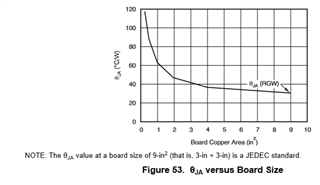
A question: the TPS7A94  datasheet does not provide a specific amount of copper needed for thermals so the device runs cool enough to hit the current spec. 

The TPS7A94EVM-046 board has quite a bit of copper on it.  Seems like all four layers are part of the thermal reduction strategy.

The EVM board measures 2.85 x 3.35 inches, so this is 9.55 in^2.  

Is there a guideline for the amount of copper needed for a smaller board? Would an amount of half the EVM be sufficient or is it another scaler factor?

dennis brown


  • Hi Dennis,

    The EVM was designed primarily to act as a faraday cage and to shield any noise in the ambient environment.  Occasionally our customers will have a difficult time recreating our noise measurements as a result of something in their environment affecting the measurement, and because the TPS7A94 is the lowest noise LDO ever created, I did everything I reasonably could to make the EVM noise immune.  A nice side effect of this shielding is the copper for thermal spreading. 

    Our thermal metrics are calculated in accordance with the JEDEC standard (2s2p) but in many cases users will apply more copper than a 2s2p design.  Increasing the PCB copper will reduce the thermal resistance until you reach what is called a "thermally saturated" design.  The following application note provides additional information you might find helpful.  The EVM is probably close to a thermally saturated design so additional steps would be necessary to cool the TPS7A94, such as forced air cooling or heat sinks applied to the PCB (such as a metal chassis which connects closely to the LDO via exposed PCB copper).

    https://www.ti.com/lit/an/spra953c/spra953c.pdf?ts=1669656889240

    In practice you can use the JEDEC 2s2p spec as a conservative value if you plan on including more copper in the PCB design, and if the calculated junction temp from this thermal resistance meets your needs, you are done.  If you need significantly less thermal resistance than the JEDEC 2s2p, you should move towards a thermally saturated design.  I would try to perform a thermal simulation on the PCB if you have the software to do this.  Alternatively you can take a measurement on your prototype of the actual thermal impedance using this app note:

    https://www.ti.com/lit/an/slva422/slva422.pdf

    Thanks,

    Stephen

  • Thanks for the reply Stephen.  

    I have three of the TPS7A94 on a circuit board that is roughly 1" x 3" (more specifically 0.7" x 2.7") .  The devices were chosen for the noise characteristics (or lack of).  In any case they are running very toasty.  The PCB is 6 layers with two layers (I believe 1 oz Cu) dedicated to ground.  While there may be other metal that does help with heat spread ultimately there is not enough of it to really help here.  This is my rationale for asking if there was a guideline for how much copper one should need on a PCB with this device.  The EVM for this device is a relatively big board in comparison.  I do appreciate that the EVM has a lot of copper for noise suppression but it does help with thermals as well.  In terms of my layout out there are three parts on one side of the shorter board edge. 

    I don't have any measurements yet for current draw for the three devices but I don't think the application is drawing the part limit of 1 amp.   A heatsink may be possible but these are pretty small parts so I am skeptical of success.  I do think they would work but there may be size constraints since the boards are pretty small.  In the past TI did publish guidelines for amount of copper area needed for certain footprints of devices.  Maybe there is one for this pkg as well?

  • Hi Dennis,

    Ah, if I understand you correctly, you are looking for something like this plot (this is not for the TPS7A94, it is taken from the TPS7A8300 and just to be used here as an example):

    If you need something like this for the TPS7A94, I can submit a thermal modeling request to have it generated.  The cycle time for these requests is 2 weeks.  Let me know if this will work and I'll submit the paperwork.

    Thanks,

    Stephen

  • Hi Stephen,

    I didn't know that TI had a page for this but here is the TI thermal calculator, are you saying that the TPS7A94 is not loaded into this database?

    https://www.ti.com/design-resources/design-tools-simulation/models-simulators/pcb-thermal-calculator.html

    Maybe I am wrong but it seems that the TPS7A94 pkg is unique here in that there are no other devices are available in the WSON 10 pin DSC pkg?  I would be ok using a close enough design to get an approximation. Something in 12 pin, etc that is similar would be ok.  

    It seems on my end that there is not enough copper to handle the heat and and is just a matter of trying to improve this.

    This is a screenshot of the devices on the board.  With three of these in such a small space the thermal part is complicated.

    I would be ok with the thermal modeling submission request. 

    For the immediate future I am really just looking for confirmation that yes, not enough copper exists here and  that is a part of the focus.  Without a change in board size it is either use a fan or heatsink.

    dennis brown

  • Hey Dennis,

    You are correct, the TPS7A94 is not loaded into that tool.  As you can see, when you search for "TPS7A" and review the available options, the TPS7A94 is likely too new to be in the tool.  I'm not aware of any approximations with other LDOs that could be used.  A couple of other new devices are also not here (TPS7A57 for instance).  I will submit a thermal modeling request to get this into the tool.

    You are correct that you need additional copper for heat spreading if your design is getting too hot.  You have what appears to be 2 large holes, if those are standoffs you might try changing them from acrylic to a metal standoff.  If they are bolt holes then it would be interesting to see if the problem goes away when the PCB is screwed into the metal chassis.  Either option will add more metal without changing your design but it does not appear that GND is connected to the holes, so you'll want to do that if possible.  I think connecting these holes to GND on both sides of the board and then to chassis or even metal standoffs will help you here.

    I would try to layout a solid GND plane from top to bottom and as much additional ground copper as possible.  You want this on both sides of the PCB as the outer layers radiate heat but the inner layers just spread it around.  I have read that matte black solder mask radiates heat better than other colors, but I have not completed any scientific experiments studying this - its something you may wish to look into and there are resources on this on the internet.  I would expect the LDO in the center to be slightly hotter than the ones on the outside, especially if you can use a metal standoff or bolt the PCB to a metal chassis with those holes. 

    Thanks,

    Stephen

  • Hi Stephen,

    Those two holes are plated through but not connected to any layers.  This is something I am looking into.  Otherwise, I would agree that the screw would become a thermal path and help a bit.  I will have to do an experiment or to.

    Interesting mention about a matter solder mask.  I will have to see if this is a possibility.  Nothing replaces have a lot more metal to deal with heat being carried away. 

    Thanks for the help.  I think we can close this out.

    dennis brown

  • More option can be done - Use metallic PCB for LDO area, Solder input and output pins to base board. It will take care of heat provided that single side PCB is ok for layout.