This thread has been locked.

If you have a related question, please click the "Ask a related question" button in the top right corner. The newly created question will be automatically linked to this question.

LM3478: The LM3478 is not working properly on heavy loads

Part Number: LM3478
Other Parts Discussed in Thread: LM348

Hi,

I am an embedded developer at Thornhill Medical, a company that makes life support devices for military applications.

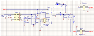
We are currently using the LM3478 IC on of our product as a Flyback power supply (see attached schematic). Recently we built three prototype boards and noticed that out of two of the three boards, the IC U2 (LM3478) is unable to generate the 5V & 12V rails when plugged into the whole system, to be more precise the 5V rail latched at 3V and the 12V rail at 8V. We did a preliminary investigation to ensure that the input voltage going to U2 is stable and found that the input voltage coming from a battery was solid and around 4.0V.

We then tried to replace the IC U2 on the board and after retesting we found out that the problem disappeared and the 5V & 12V rails were available when the board was plugged into the whole system.

Can you please help us identify what would have caused U2 IC to work partially and what can be the potential reason for U2 to get damaged and then work partially?

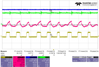
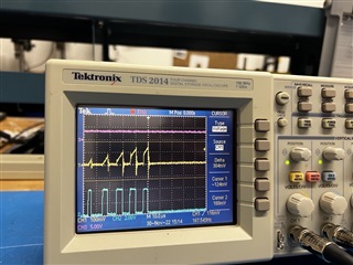
For providing some more details, I am also attaching some oscilloscope screen shots of the IC when it is working under lighter loads

CH1- Gate drive input to mosfet Q3

CH2 - Voltage measured on sense resistor R11

CH3 - 5V rail on the coupled inductor coil 4-5

CH4 - Input voltage coming from battery (5VPWR net in schematic)

We are hitting our deadline in delivering this build and would like to understand the reason for the fallout for U2 before we can proceed to build more units.

Kindly provide us with some guidance into our issue and hoping to hear back from you by end of this week.

Regards,

Nihar Joshi

  • Hello Nihar,

    The measurement of the voltage on R11 looks not as expected. Normally you should have triangular waveform when the transistor is conducting and GND when the transistor is off.

    Please check your layout according the layout guidelines in chapter 10 of the datasheet. It is important that you route the high power routes far away from the sensitive nodes.

    Especially use 2 separate nets for AGND and PGND and a net tie to get them together at the IC. Otherwise it is really hard to make sure that you do not mix them.

    How did you calculate the compensation? I am asking as I do not like the change in on-time that I can observe in your design.

    For a review of the schematic, I need at least the parameters:

    VIN min and max

    VOUTx ripple target

    IOUTx

    Which transformer are you using? Please check the signals on all pins during startup and in normal operation. This should give some more hints to identify the root cause of the damage.

    Best regards,
    Brigitte

  • Hi Brigitte,

    Thank you so much for your response. I have some update from my testing yesterday that I would like to share with you. Basically now I don’t feel like the IC was ever damaged in the first place and just that the design is marginally working with them.  I will explain this further:

    Our design is a 2-layer board and we had made some copper updates recently to add some additional circuits for protecting the battery from extreme temperatures during charging and discharging. Although these additional circuits have been disabled at the moment, but they do occupy real estate on the board and have replaced some of the ground pours that used to exist before.

    Yesterday I replaced the non-functioning IC from the new revision of the board with the copper changes mentioned above to an older revision of the board without those changes and everything worked fine which tells me that the IC populated on the new revision of the board was not damaged.

    I have some more screen grabs of the oscilloscope that I took yesterday using the new revision of the board when the system was working  and also screen grabs when the system was not working. The only difference in going from a working state to non working state was the swapping of LM348 IC’s.

    Fig1 (When the system is working)

    Fig2 (When the system is not working)

    Fig3 (When the system is not working)

    Regarding your questions related to the design, I will review the system requirements and get back to you on that.

    Regards,

    Nihar

  • Regarding the transformer we are using, its a custom made transformer. I am sharing the pdf of the bobbin used for it and the instructions for building it.

    • The inductance between pin 4 and 5 is 3.6uH +/-1uH
    • The inductance between pin 3 and 7 is 20.4uH +/-5 uH
    • The inductance between pin 1 and 9 is 0.7uH +/-0.2uH

    122360-A.pdf124800-B.docx

  • Hi Bridget,

    The parameters that you requested are:

    VinMax -4.2V, VinMin-3V

    Vout(ripple target for the 5V rail)- 100mVp-p (max)

    Iout(5V rail) - 3-4 A

  • Hello Nihar,

    I expect that the basic problem is your GND connections. If the system is working properly with a good GND connection, I think it makes most sense to improve the GND connection instead of trying to solve a layout induced problem with changing anything else in the circuit.

    Best regards,
    Brigitte