This thread has been locked.

If you have a related question, please click the "Ask a related question" button in the top right corner. The newly created question will be automatically linked to this question.

TPS62130A-Q1: Converter output problem

Part Number: TPS62130A-Q1

Hi Team, 

Good day. I am posting this inquiry on behalf of the customer.

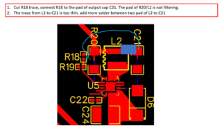
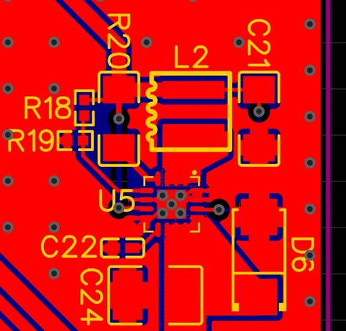
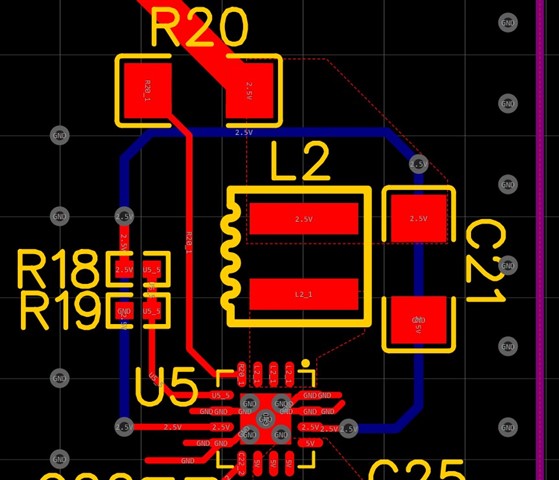
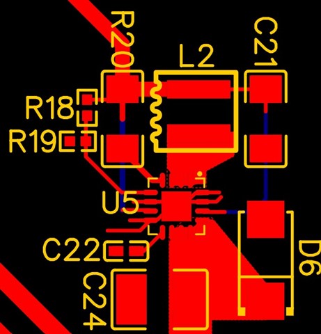
"I encountered a problem with my 2.5V DC converter (see U5). The input is 5V with an output of 2.5V. Currently, the prototype is not output 2.5V but rather ~1.3V even though the auxiliary resistors and capacitors and layout are followed.

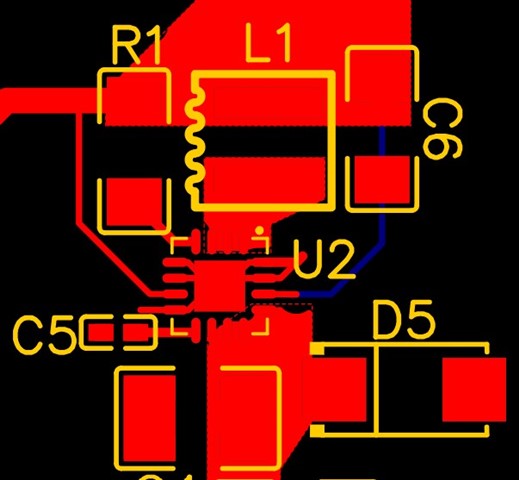
I have attached the PCB layout and the schematic of the U5 subcircuit. Red means the top layer while blue means the bottom layer.

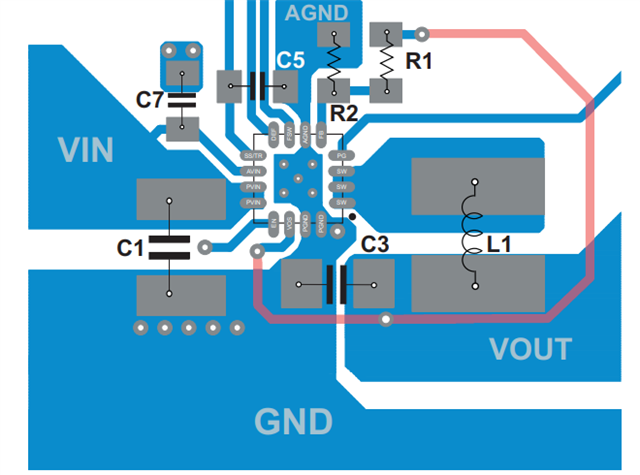
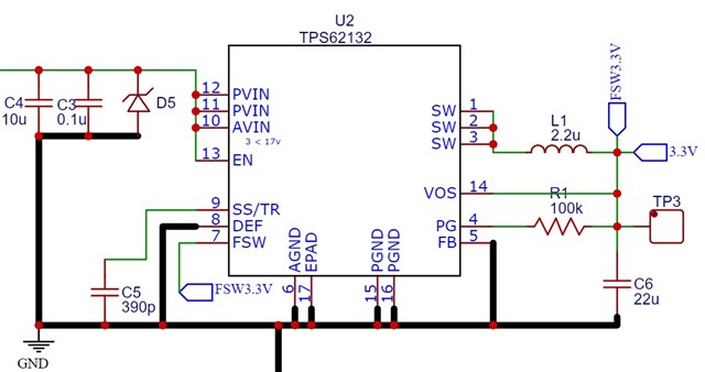
I have also attached the PCB layout and schematic of my 3.3V DC converter (see U2) for your comparison. I included this comparison since the auxiliary components are similar and the PCB layout is similar. The good thing about U2 is that this converter works."

The ground areas of the PCB layout are hidden. The red copper traces that look like dead ends are actually connected to the bottom GND plane.

Please help to advise. Thank you for extending your support.

Kind regards, 

Marvin

  • Hi Marvin,

    Do you know what the input voltage and output current are for these converters?

    I would also ensure that the boards are clear of any flux buildup, especially near the feedback resistors.

    For the layout I would recommend having the input and output capacitors share ground connection closely as in the example layout in the datasheet.

    The output capacitor should be connected through a Vout plane to the inductor, skinny traces connecting the inductor and output cap could cause a larger voltage drop. 

    In addition, take the FB signal from the output capacitor similar to the layout below. 

    You might check to see if the customer can send a picture of their layout with the GND planes shown.

    Thanks,

    Joseph

  • Hi Marvin,

    Please see my comments on U5 layout. Hope this helps,

    Thanks,

    Nancy

  • Hi Joseph, Nancy,

    Thank you for your prompt response. Please see the feedback from the customer.

    1. For both the 2.5V and 3.3V converters, the input voltage is 5V and the output current is <1A.
    2. There is no visible flux buildup on the board after prototype fabrication.
    3. I will revise the common ground connection between the input and output capacitors since in the layout the TVS diode intersects them.
    4. Thank you for clarifying this. I will remove the thin trace for the VOUT plane. Maybe this is the reason why the 3.3V converter works but the 2.5V one doesn't.

    5. What does "The pad of R20/L2 is not filtering" mean? Is this a bad thing? How should I resolve this?
    6. I have attached pics showing the ground plane for the U5 subcircuit

    Please help to advise. Thank you for extending your support.

    Kind regards, 

    Marvin

  • Hi Marvin,

    5. The pad of R20 and L2 which connects to R18 is before output capacitor C21. It is very noisy and the noise may couple into feedback pin. The feedback resistor R18 should be connected on the pad of output capacitor C21 directly for accurate output. Also please deep clean(brush) the board using alcohol or drop the board into an ultrasound cleaner for 15 minutes. Sometimes, the flux contamination may not be visible. But it is on the board. Have a try.

    Thanks,

    Nancy

  • Hi Nancy, 

    Thank you for the response. Please see the feedback from the customer.

    I have attached a screenshot of my revised PCB layout.

    I have attached the feedback resistor R18 directly to the output capacitor C21. However, I am not sure about my decision to connect the FSW pin to the feedback resistor R18 as well. It creates a semi-circle on the bottom layer (color blue) and I am not sure if this is bad or not (altho the datasheet didn't say anything about this). Hence, I would like the team to inspect the FSW pin PCB layout as seen in the screenshot.

    The dotted lines in the screenshot signify a hidden copper area.

    Please help to advise. Thank you for extending your support.

    Kind regards, 

    Marvin

  • Hi Marvin,

    I would recommend that the customer connect FSW pin directly to VOUT instead of on the FB path trace. The reason is that there will be a small leakage current through this pin that we want to make sure doesn't affect the FB signal. 

    Thanks,

    Joseph

  • Hi Marvin,

    I agree with Joseph, please connect FSW pin to the pad of C21 directly. Did customer fix or improve the issue for 2.5V by adding solder on the pad of C21 and L2?

    Thanks,

    Nancy

  • Hi Joseph, Nancy,

    Thank you for your response. Please see the feedback from our customer.

    "I have followed the PCB layout from your latest comment. I've also decided to look at a voltage reference IC rather than a DC converter for my design (as seen in my current case CS1447901). Please inform the product team of this and I thank you both for your support! You may finally close this case."

    Thank you for extending your support. Your help is much appreciated.

    Kind regards, 

    Marvin