This thread has been locked.

If you have a related question, please click the "Ask a related question" button in the top right corner. The newly created question will be automatically linked to this question.

Power protection for Automotive electronics

Other Parts Discussed in Thread: LM7480-Q1, LM5060, LM74800-Q1, LM74700-Q1, LM74722-Q1, LM74721-Q1, LM74720-Q1, LM5175-Q1, LM74800EVM-CS, LM7480

Hello There,

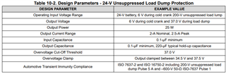
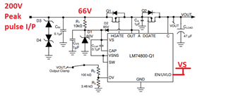
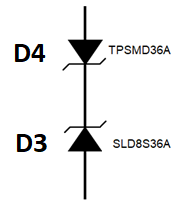
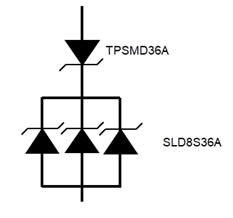
We are designing a new product for automotive applications (like ECUs) that is powered by a 12 or 24 V battery, and our application requires 15 A of current. Could you please suggest any power protection techniques that could help our product clear load dump, reverse voltage protection, and superimposition of AC tests?

Thanks,
Sakthivel

  • Hi Sakthivel,

    Our ESD/Surge protection devices can protect from transient events, however we don't have any devices that can withstand 15 A of current for 12/24 V battery systems.

    It sounds like you're looking for a power switch, something like the LM7480-Q1, however I'll loop in the correct experts to comment.

    Regards,

    Sebastian 

  • Hi Sebastian,

    we found Automotive 12- and 24-V Battery Input Protection IC "LM5060" which compliance both ISO 7637-2, ISO 16750-2 but the part and FETs used are not available, could you please provide alternate part for LM5060?  if possible please share it with over current protection.

    Thanks,
    Sakthivel 

  • Hi Sakthivel,

    LM74800-Q1 fits here. Please refer Section "10.3 200-V Unsuppressed Load Dump Protection Application" in the LM74800-Q1 data sheet and let us know if you have any questions.

    Best Regards,

    Rakesh

  • Hello Rakesh,

    The part needs mere room it seems, by having too many diodes , FET and bulk capacitors and few components are not available in stock, Is there any single Chip solution with few FETS and bulk capacitors for Automotive input protection systems? 

    Our requirement:

    1, Input Voltage : 9 to 36 V.

    2, Current : 15A if 9V input and 4.5A if 36 V input.

    3, Temperature range : -30 to 70 Deg celcius

  • Hi Rakesh,

    This is LM5060 based protection circuit, "https://www.ti.com/lit/ug/tiduc41/tiduc41.pdf"

    1, why do we need two FETs ? Can we skip the NPN transistor part ?

    2, Can we skip the Enable circuit part also?

    Thanks,  

  • Hi Rakesh,

    please find the simple Block diagram of our Automotive product, as per our understanding the power protection should be compliance to ISO 7637-2, ISO 16750-2, which includes load dump test, Reverse voltage protection, and Super imposition of AC voltage test etc..

    1, Does our system requires all those tests?

    2,  Does LM5060 /LM74800-Q1 compliance to Super imposition of AC voltage test?

    3,- Could you please suggest any battery input protection methods for our system?

    Thanks

  • Hi Sakthi vel,

    LM5060 is not suitable for this application as it does not have reverse current blocking functionality which is required to rectify AC Super imposed voltage.

    The devices which can support all your requirements are (ISO 7637-2, ISO 16750-2, which includes load dump test, Reverse voltage protection, and Super imposition of AC voltage test)

    1. LM74700-Q1 (This device drives only ideal diode FET and can be used if forward current blocking is not required.)
    2. LM74800-Q1, LM74801-Q1, LM74810-Q1
    3. LM74720-Q1, LM74721-Q1 and LM74722-Q1

    For more understanding on battery input protection, please refer to Application Note - Basics of Ideal Diodes

  • Hi Preveen,

    Thanks for your support,

    Please find the simple power flow diagram of our product, kindly review it, and let us know if there will be any issue by connecting "LM7480X-Q1" and "LM5175-Q1."

    we planned to use the following power protection ICs based on the availability "LM7480X-Q1, LM7481X-Q1"

    Thanks,
    Sakthivel

  • Hi Sakthivel,

    The block diagram looks good to me.

  • Hi Praveen,

    In the Lm7840 datasheet, we are able to see only 2V peak to peak AC superimposition suppression; is it possible, with the LM7840 or LM7841, to superimpose AC up to 10V peak to peak as per the standard of ISO 16750-2?

    https://www.compel.ru/wordpress/wp-content/uploads/2017/05/ISO-16750-22010E-.pdf

    Thanks

    Sakthivel

  • Hi Sakthivel,

    Yes, there should be no issue in rectifying 10V pk-pk AC super imposed signal. The frequency of the AC signal is important parameter to know if the Ideal Diode controller can rectify the signal or not. Please refer to the Ideal Diode Controllers for Active Rectification of AC Voltage Ripple application note for more understanding.

    Please note that the charge pump currents of LM74800-Q1 and LM74810-Q1 are wrong in the application note table 1. I have updated the correct values in the snapshot below. You can calculate the correct 'Maximum Gate Charge QGM at AC ripple frequency FAC' value by using the equation (1).

  • Hi Praveen,

    What is the maximum output current can be driven from LM7480x ? 

    Output current range specified in the table -> 2A for 24V load, Is this only for example ?  

    Our product requires 150W of power so roughly 6A required if input voltage in24V will LM740x capable for handling such loads?

    Thanks,
    Sakthivel

  • Hi Sakthivel,

    The application example in the datasheet is just an example. There is no load current limitation with LM7480-Q1 as this device is just a controller and the load current is carried by the external FETs. As the load current increases, you will have to use FETs with lower Rds(on) FETs or use more number of FETs in parallel to spread out the power dissipation and thermals.

  • Hi Praveen,

    If the part "LM7480-Q1" is used in the common source configuration for 200V load dump suppression as mentioned below,

    Will it be capable of rectifying the superimposed AC voltage for a 24 V system? with 6V peak-to-peak?

    In the design parameter of the 24V unsuppressed load dump protection table, we don't find information regarding superimposed AC voltage.

    If the part is not suitable, how do we achieve the power protection with 200 V of unsuppressed load dump, reverse power protection, and superimposition of AC voltage?

    Thanks,

    Sakthivel

  • Hi Praveen,

    Please suggest any 200V Hgate FET parts,

    Thanks,
    Sakthivel

  • Hi Sakthivel,

    In LM74800EVM-CS we have used IPB320N20N3. The FET you require may be different depending on your load current. For detailed FET selection guidelines please refer to '10.3.2.5 MOSFET Q1 Selection' section of datasheet. 

    ... 

  • Hi Praveen,

    As per our understanding, we are able to protect a 200V load dump with the common source configuration, so we plan to proceed with the CS configuration. Could you please ensure that with the CS configuration we can achieve the listed protection features?

    1, Rectifying superimposition of AC 6V peak to peak with upto 200KHz frequency?

     -> we dont find an appropiate data for LM7480 can rectify 200Khz AC in Common source configuration.

    2, What could be the maximum reverse voltage can be blocked by LM7480 in Common source configuration,

    Thanks,

    Sakthivel

  • Hi Praveen,

    We can find the AC super imposed test data only for Common Drain configuration (12V system) in the table 10.1 (LM7480-Q1 data sheet)  

    As mentioned previously, our requirement is that our project should withstand 200 volt load dump test hence we need to choose common source configuration. for 24V battery system, but in datasheet the 24V domain specification table does not have any data regarding AC superimposition 

    1, Could you please ensure the the part with common source configuration can rectify the superimposed AC voltage?

             If so please provide us the till what frequency and magnitude rectification is possible. 

  • Hi Sakthi vel,

    The AC super imposed signal rectification capability of a controller depends only on its Charge Pump source current (I(CAP)) strength. The rectification capability does not depend on the FET configuration - common drain or common source. 

    Please refer to the Ideal Diode Controllers for Active Rectification of AC Voltage Ripple application note for more understanding. Please note that the charge pump currents of LM74800-Q1 and LM74810-Q1 are wrong in the application note table 1. I have updated the correct values in the snapshot below. You can calculate the correct 'Maximum Gate Charge QGM at AC ripple frequency FAC' value by using the equation (1) below.

  • Hi Praveen,

    Based on our understanding, we are going to draft the schematics as shown in Figure , with the parts mentioned below, Our expectation of the part's behavior is to withstand the following conditions, kindly review and give your feed back.

    1. As per the test, our device must withstand 200 V load dump pulses for duration of 350 ms for 5 cycles.

    2. The part should rectify the AC superimposed voltage with a magnitude of 6 volts peak to peak at a frequency of 200 kHz.

    3, The part should block the reverse voltage of -35V.

    4, Output should be clamped to 37V if input is 200V peak pulse.

    Sno Reference Desig Part Number Remarks
    1 D4 Bidirectional SMBJ30CA Breakdown Voltage - 33.30V
    2 D3 Uni Directional SMBJ30A Breakdown Voltage - 33.30V
    3 Q1, Q2 Mosfet BSC117N08NS5ATMA1 Total Gate Charge18 nC @ 10 V Vgs Th

    Thanks,

    Sakthivel

  • Hi Sakthivel,

    1. D4 needs to be SMBJ33CA
    2. D3 can be a normal diode or TVS diode with a minimum reverse breakdown voltage of 150V.
    3. Q1 needs to 200V rated FET.
  • Hi Praveen,

    Thanks or your support,

    As per our understanding, the TVS diodes are used to clamp the input voltage; if the input exceeds 65, it will clamp, and since it is bidirectional, if reverse voltage occurs, it will direct it to the battery and protect the circuit. Please ensure our understanding is correct.

    1. We chose the TVS diodes and wired them together as shown in the figure: D4 - "TPSMD36A"; D3 - "SLD8S36A" (D3 and D4 have a clamping voltage of 53 volts).

    If there is an input load dump (202V peak pulse voltage), the D3 TVS diode clamps it to 53V, and if the reverse voltage exceeds -53V, the D4 diode clamps it to -54V, and the LM7480-Q1 protects the circuit until the reverse voltage is -53V. Is our interpretation correct? If this point is correct, we don't need a 200-volt-rated MOSFET for HGATE, right? The total gate charge of currently available 200V-rated FETS is 30nC, and only a very low frequency of AC super imposition can be rectified. For that only, we decided to go with 100V-rated FETS,

    2. For example, if the total gate charge of the FET is 25 nC, then the maximum frequency of AC superimposition that can be rectified by our part is 108 kHz if the charge pump current is 2.7 mA. Is this understanding correct?

    Thanks,
    Sakthivel

  • Hi Praveen,

    Is there any update on the below request?

  • Hi Sakthivel,

    The duration of load dump can be for 400ms. The TVS will not be able to clamp the voltage to a lower level as you mentioned due to the limitation of its power rating. Hence we have to use the Common Source topology of LM7480-Q1 with 200V rated FETs.

    You can consider using LM74810-Q1 which has higher charge pump source current which helps in rectification of higher AC superimposed frequency. 

  • Hi Praveen,

    1, Can i connect the diodes as shown in the below image for withstanding 200V load dump for the duration of 400mS ?

    2, Can we use the  "LM74810-Q1" for 200V load dump case? in front of the diode structure mentioned in the image ?

                    Because nowhere in LM74810-Q1 data sheet it is mentioned that we can use the part for 200V un suppressed load dump protection.

    3, Does all other functionalities of LM74810-Q1 is similar to LM7480 ? 

  • Hi Praveen,

    Is there any update?

  • Hi Sakthi vel,

    All the functions of LM74800-Q1 and LM74810-Q1 are similar expect for the higher charge pump source current strength of LM74810-Q1. So, LM74810-Q1 can be used in common source topology to protect from 200V un-suppressed load dump pulse.

    Regarding connecting TVS diodes in parallel, you will have to verify if the TVS diodes have enough peak pulse power rating for 350ms-400ms.  For the TVS diode selected, I see that the peak pulse power vs pulse width information is available only up to 100ms. So, we will not be able to comment if the 3 TVS diodes connected in parallel will help clamp the 200V un-suppressed load dump pulse.

    Also, please remember the below points while calculating for the input TVS power dissipation,

    • It is important to know the input impedance of the 200V un-suppressed load dump pulse which is applicable in your system. As per ISO 16750-2 the input impedance can vary from 1Ω to 8Ω. Lower the input impedance, higher the power dissipation in the TVS while clamping.
    • you will have to derate the peak pulse power for maximum junction temperature as well.