This thread has been locked.

If you have a related question, please click the "Ask a related question" button in the top right corner. The newly created question will be automatically linked to this question.

TPS54360B: Load Dump Protection using SNVA681A – March 2015 Reference Design

Part Number: TPS54360B
Other Parts Discussed in Thread: LM5088,

Hi Team,

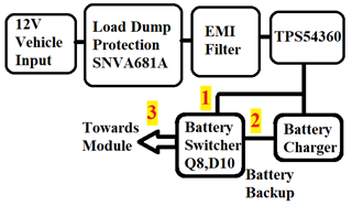
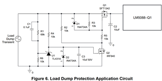
I intend to use the reference design mentioned in the document (1) SNVA681A – March 2015, page no. 5

Figure 6. Load Dump Protection Application Circuit, attached the image for reference.

Instead of LM5088–Q1 I am planning to use the TPS54360B.

Here my question is,

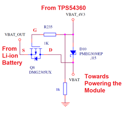
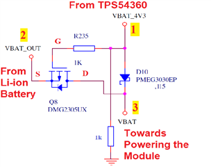
Q1. As a P channel MOSFET is used on the high side,

should we not connect the Drain of P-MOSFET towards the source side 

and Source of the P-MOSFET towards the load side (LM5088–Q1)?

The reason I need clarification is because in the reference document (2) Automotive MOSFET Reverse Battery Protection,

that is the recommended orientation for the P-MOSFET on high side.

Also when we refer (3) 17TIDUC42 – November 2016,

the N-MOSFET orientation is same as mentioned in the document (2) for N MOSFET.

Q2. So should we not follow the same P-MOSFET orientation as mentioned in (2) for the circuit diagram mentioned in Figure 6?

Kindly clarify.

Reference Link:

1. SNVA681A – March 2015:

https://www.ti.com/lit/an/snva681a/snva681a.pdf?ts=1670958866754&ref_url=https%253A%252F%252Fwww.google.com%252F

2. Automotive MOSFET Reverse Battery Protection

https://www.infineon.com/dgdl/Reverse-Batery-Protection-Rev2.pdf?fileId=db3a304412b407950112b41887722615

3. 17TIDUC42 – November 2016

https://www.ti.com/lit/ug/tiduc42/tiduc42.pdf?ts=1670920446323&ref_url=https%253A%252F%252Fwww.google.com%252F

Thanks in advance!

Warm regards

  • Hi Swaroop

    I think in the Publication2 and 3, you are referring to a Reverse polarity protection reference. While in Publication1 , is a Load-dump protection application circuit. That's why there is  difference.

    Thank you.

  • Dear Gui He,

    Thanks for your quick reply. Yes I do agree that both the end use application is different.

    What I intend to verify is the circuit below:
    I wish to use a P-MOSFET to switch to battery power when power from TPS54360B is absent using this circuit:

    So in the schematics above, kindly help me verify the correct orientation of P-MOSFET?
    should the Source be connect to the battery or at the cathode of D10 ?

    I fear that the body diode might lead to leakage current flowing into the battery, ends up damage the battery.

    Thanks a lot for your support.

    Warm regards

  • HI 

    can you show more specific connection way, the Li-Ion battery is output of TPS54360B or input of TPS54360B? 

    if the body diode is block the current from input source to DCDC, it is used to disconnect the input source and dcdc.

    if the body diode can't block the current from input source to DCDC, it is used to block the reverse voltage 

    Thanks

  • Dear Daniel Li14,

    Thank you for your feed back.

    Kindly find the schematics parts:

    Power flow is given below:

    Vehicle battery 12V -> Load dump protection -> EMI Filter->TPS54360->Battery Charger and Battery Switcher (Q8,D10) -> Module

    Battery Switcher gets active only when vehicle battery is absent.

    1,2 and 3 are:

    I want fast switching of Q8 during vehicle battery disconnect,

    and battery should supply module.

    Thanks for your support.

    Warm regards

  • Hi

    you need move D10 between S and G of Q8. when Node 2- Node 1 voltage higher than Vgth of Q8, it will connect node 2 and node 3. it the voltage between Node 2 and  Node 1 less than Vgth of Q8,  node 2 and node 3 will be disconnect. see below simulation, Vg th=-2.5V

  • Dear Daniel Li14,

    Thank you for the explanation and sharing the simulation results.

    I wanted to know more about the function and use of the body diode on the P-MOSFET.

    can you share some information on the body diode of MOSFET.

    thanks for your support.

    Thanks and regards

    Swaroop

  • HI

    I am not very clear about your question. No Matter the p-mos is on or off, the diode always conduct when Drain to Source have positive voltage.  so if you want to use as the mosfet as a switch to disconnect from source to load, the Source Node need to be connect to input side, and the Drain Node need to be connect to output side to avoid the body diode conduct. 

    Thanks

  • Dear Daniel,

    Thank you so much for your reply!

    This resolved my issue!

    Best wishes thanks!