This thread has been locked.

If you have a related question, please click the "Ask a related question" button in the top right corner. The newly created question will be automatically linked to this question.

TPS54202: Extra noise and ringing

Part Number: TPS54202
Other Parts Discussed in Thread: TPS562201, , TPS54308, TPS562208

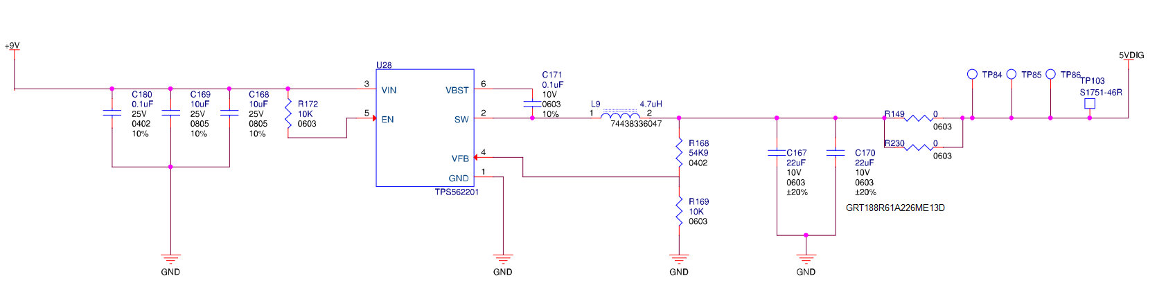
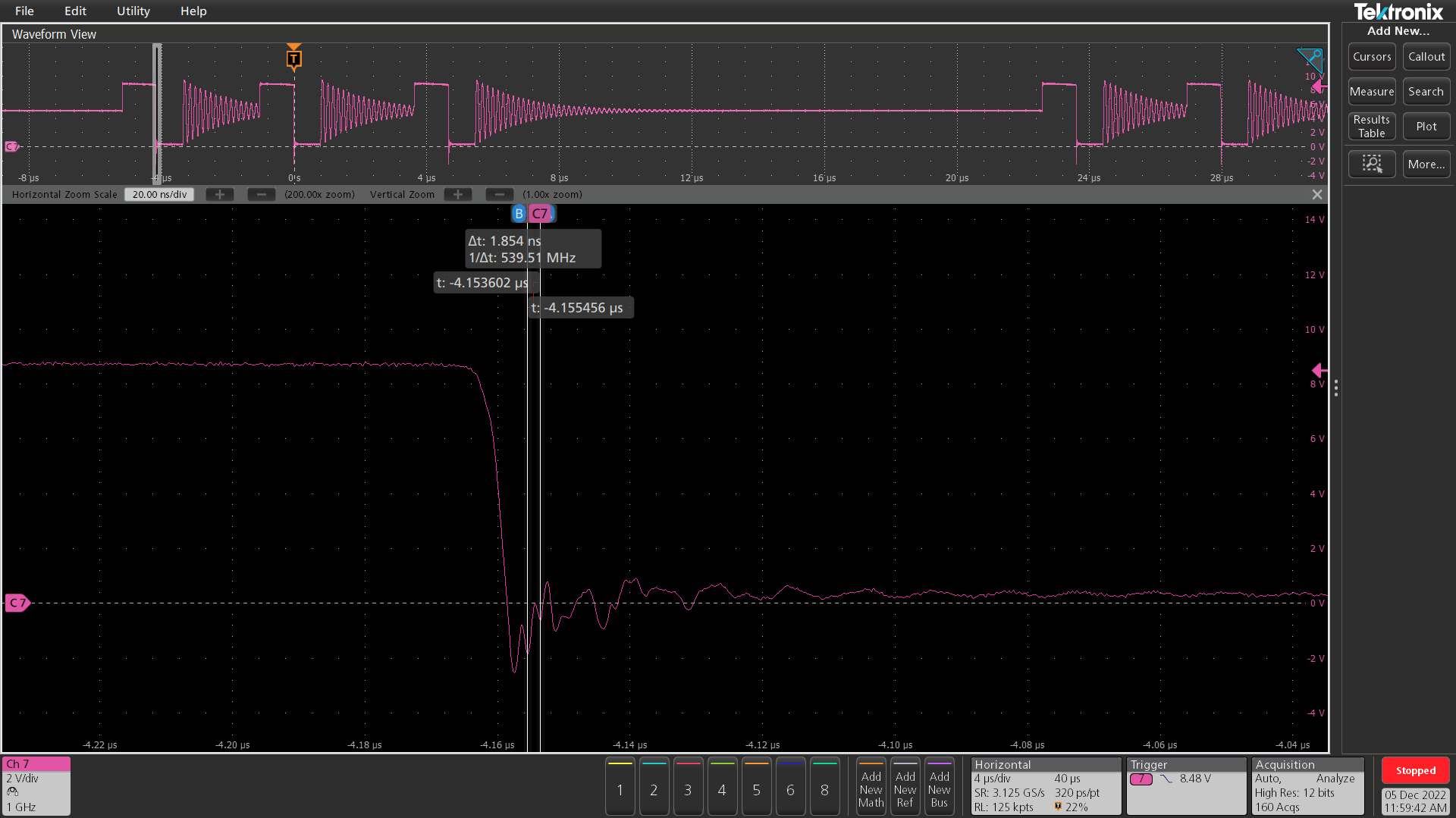
Team, I have a customer experiencing noise on the switch node of the TPS562201 and they are now seeing the same behavior with the TPS54202.  Can you offer any advice to help supress this?  Ideally, we can maybe beef up the switch node with a white wire or add a snubber circuit to test on the existing board to give confidence in a solution.  We have the opportunity to change the PCB, so if there is a better device that offers low EMI and good efficiency we can offer this. 

The particular circuit involved is 9V input 5V output @2A

We have recommended the same device for another rail with 9V input 3.3V output @1A.  Both of these power a noise sensitive RF node and low noise is important.  Please advise.  Thank you!

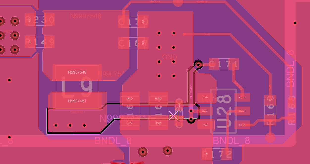
Scope shot, Layout and Schematic is attached.

L1 TOP red

L2 GND

SW node routed in L3

L4 GND

Thank you!

  • Hi Will,

    1.May i check what nosie you are talking about ? The wavefroms seems device is not stable at this application .

    2.What's the loading of the SW waveform you captured ? Pls note that TPS54202/TPS562201 is a ECO mode part that means it will enter PFM mode at light load. If you need convertor works in CCM mode at all loading , better to select a FCCM part like TPS54308, or TPS562208

    3. For TPS54202, pls remove the R172 if no need to adjust the EN threshold voltage , it may damage EN PIN as EN pin abs voltage is only 7V. Or you can add one more resistor in chapter "7.3.5 Enable and Adjusting Under Voltage Lockout"

    4. Regarding layout, You can enlarge the GND Polygon as large as possible to surround the component and IC, and place more VIAs near IC to bette thermal performance .