Because of the Thanksgiving holiday in the U.S., TI E2E™ design support forum responses may be delayed from November 25 through December 2. Thank you for your patience.

This thread has been locked.

If you have a related question, please click the "Ask a related question" button in the top right corner. The newly created question will be automatically linked to this question.

TL494: TL494

Part Number: TL494
Other Parts Discussed in Thread: TL598

Hi all the team members,

We are using TL494 IC for some specific applications. We need small information about TL494.
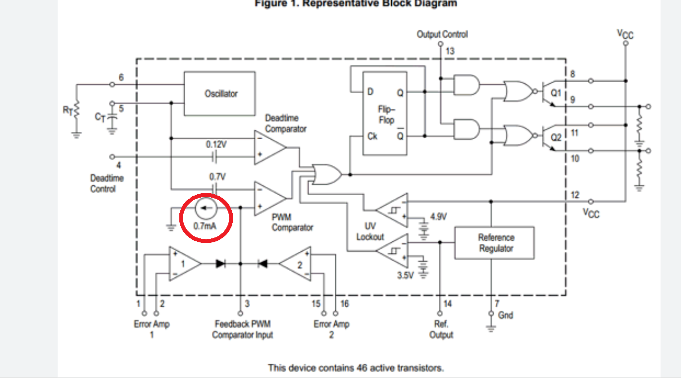
The above picture is block diagram of TL494. In that picture i marked 0.7mA with red color.

So i want to know about functionality of that particular amount of current and importance. 

will u possible to use TL494 for average current mode controller or not?

  • Our office is currently closed for the US year end holidays. We will reply to your request shortly. 

    Best regards, 

    Don

  • Hello, Santhosh,

    0.7mA sink current is used to pull the amplifier output low to provide maximum pulse width out when both amplifiers are biased off.

    TL494 is intended for voltage mode control. 

    Regards,

    Sean

  • Hi sir,

    Thanks for reply.

    I want to know about one more point about TL494.

    TL494 Internal PWM controller  whether positive feedback or negative feedback?

  • It seems negative feedback. When the voltage of Pin 3 is smaller, the output duty cycle is bigger.

  • But block diagram of TL494 when compare to TL598 then  PWM controller block of TL494  seems like positive feedback.

    Can u please show me in TL494 block diagram  how it is converted to negative feedback.

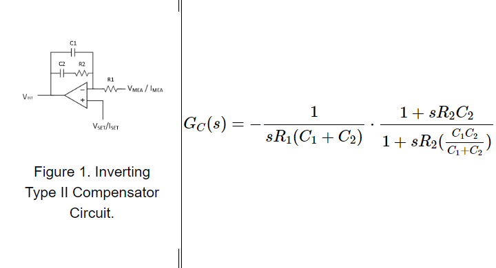
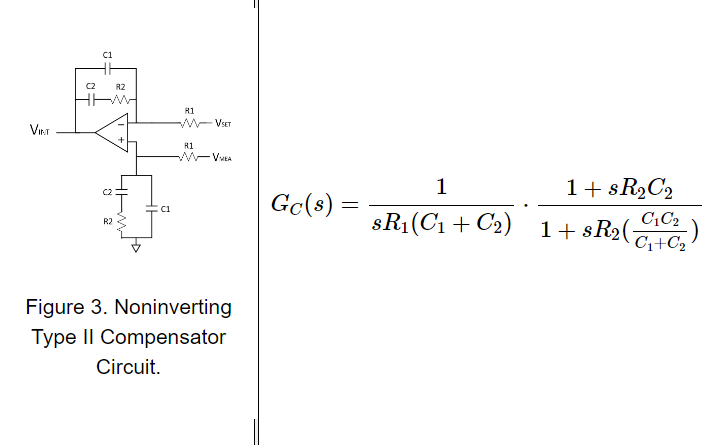
    The below figure represents non-inverting type2 compensator. But Op amp IN+,IN- the R-C circuit represents same, In inverting Type 2 they are not keeping R-C circuit like this

    Can u explain why they represent like this for non-inverting Type2 compensator.

  • Hello,

    In Figure 1, the input sensing voltage is collected to inverting INPUT, from the the level of OPAMP, it is negative feedback, and the transfer function output has minus sign;

    In Figure 2, the input sensing voltage is collected to non-inverting INPUT, from the the level of OPAMP, it is positive feedback, and the transfer function output has no minus sign;

    But from the level of closed loop, the feedback has to be negative feedback. When output is increased, the duty cycle has to deceased. Maybe the OPAMP output is increased, but the PWM COMPARITOR can decrease the duty cycle. Per my understanding, the Figure 2 is used for TL494. When OUTPUT voltage  is increased, the OPAMP output is increased, but the PWM COMPARATOR (and NPN Drive output) reduces duty cycle, and hence the output is reduced.

    I don't have more detailed internal block diagram than what is provided in D/S.

    I hope this helps,

    Regards,