This thread has been locked.

If you have a related question, please click the "Ask a related question" button in the top right corner. The newly created question will be automatically linked to this question.

TPS543C20A: TPS543C20A LOAD TRANSIENT

Part Number: TPS543C20A
Other Parts Discussed in Thread: TPS548D21

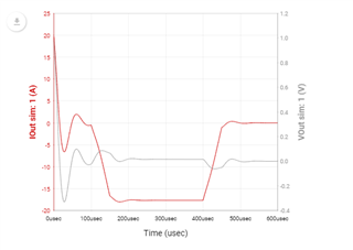
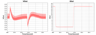
I tried to perform Load transient of any combination. Unable to get the proper waveform. Output voltage goes negative. Looks like webench model is not working. Other IC like TPS548D21, load transient works perfectly. So kindly verify load transient for TPS543C20A on your website. Also load transient pspice model is not available. Only startup and steady state model available. Kindly send load transient model. 

  • Hello Raghavendra, 

    Thanks for pointing this out 

    I run a load transient from my side and able to get the same results as yours. Peter is looking at this. 

    Thanks! 

    Tahar

  •  

    There is a transient (switching) Pspice model for the TPS543C20A available in it's product folder - https://www.ti.com/product/TPS543C20A#design-tools-simulation 

    Start-up and Steady-state describe whether the soft-start portion of the devices power-on sequence is included in the schematic model.  Steady-state models skip the soft-start start-up to speed up simulation times by starting the part already running in steady-state rather the 0V output.  Either can be used to simulate a load transient by including a dynamic load, such as a piece-wide-linear current source, or switched resistor.

    As for the WeBench simulation issue, the simulation appears to be rapidly resetting to 0V and applying a negative IOUT transient.

  • As for the WeBench simulation issue, the simulation appears to be rapidly resetting to 0V and applying a negative IOUT transient. I am not sure I got this. What can do to get a classic load transient waveform. Like shown below. Also, I have another question, is there a way to change load current slew rate.   

  •  

    I was able to get the WeBench transient simulation to run by increasing the Over Current Protection (OCP) level.  The simulation was triggering OCP and shutting the output voltage off during the 200μs before the output waveforms appeared.

    You can adjust the depth, timing, and slew-rate of the transient load current by clicking on the Pulse current source in parallel with the load resistor, and selecting "Update"

    Note:  the Current Source is in the negative polarity, so it reduces the load current from the steady-state resistive load current.

  • This waveform is not a classic waveform as compared to one i posted. Looks like lot of noise. I can not share this waveform with my customer. I need a better waveform like other TI chips do. I wonder how will be the actual performance of this IC. I am trying to simulate in pspice to better understand the IC and get classic waveform.

  •  

    The look of the waveform is a biproduct of the design parameters that were selected.  Switching at 1.2MHz, it was designed with mixed output capacitors and allowing a high output voltage ripple.  In addition, the loop's bandwidth was fast enough that the 50μs, 18A load transient produced almost no viable change in the output voltage relative to the high output voltage ripple.

    If I use the customization options to reduce the switching frequency to 600kHz, restrict the output voltage ripple to 1% (10mV) and the transient to 3% (30mV) the design produces a "classic" transient response that you are looking for.

    Similarly, if I leave the switching frequency at 1.2MHz and select 1% ripple and 3% transient, the design produces a more "classic" transient response

    It's the default 3% ripple and 5% transient design combined with mixed output capacitors that is producing a high enough output voltage ripple to mask the transient response.

  • I had to set current limit almost double the output load current to get classic waveform. Wondering actual IC also I need to design such a high limit to work or this is just simulation error.

    Also I would like to download orcad/cadence design file for PCB etc. But getting error and not able to download. Any suggestion please. 

  •  

    The current limit error is a simulation artifact of trying to start the simulation at steady-state with a very fast loop response.  Small errors in the initial conditions for some of the nodes in the feedback and regulation loop create an output voltage error, which the part has to respond to, which can create very large output voltage transients while the control loop establishes it's steady-state operating condition.

    In a real circuit, the converter ramps up with a controlled soft-start to avoid this condition.

    Regarding the Cadence / Or-CAD file, which version of Or-CAD are you trying to down load?

  • I am trying to download 17.2 version. I am getting an error message -Export failed-submit error.

  • I downloaded that version myself and did not receive an error message.  The file is attached.

    ul_TPS543C20ARVFR.zip