A related question is a question created from another question. When the related question is created, it will be automatically linked to the original question.
If you have a related question, please click the "Ask a related question" button in the top right corner. The newly created question will be automatically linked to this question.
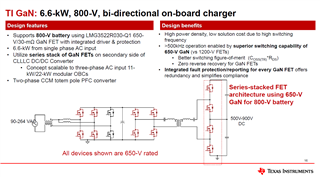
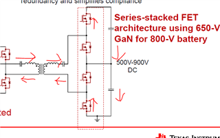
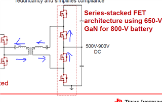
The output capacitors divide the output voltage so that no fet sees more than half the output voltage. This allows for 650V FETs to be used in an 800V application.
This design uses a half bridge output rectifier, and the current flow looks like this when sending power to DC side: