Hello,
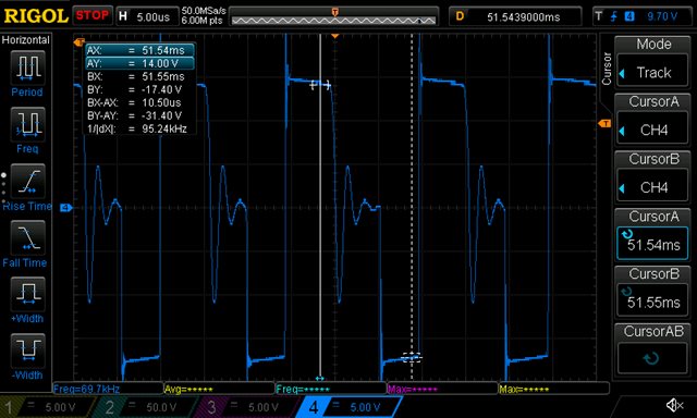
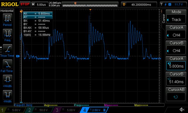
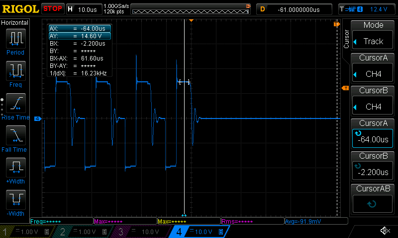
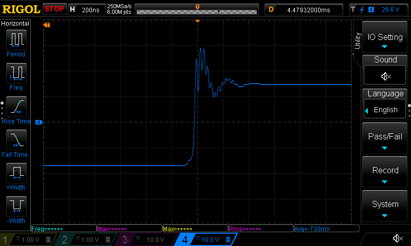
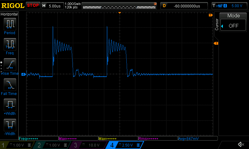
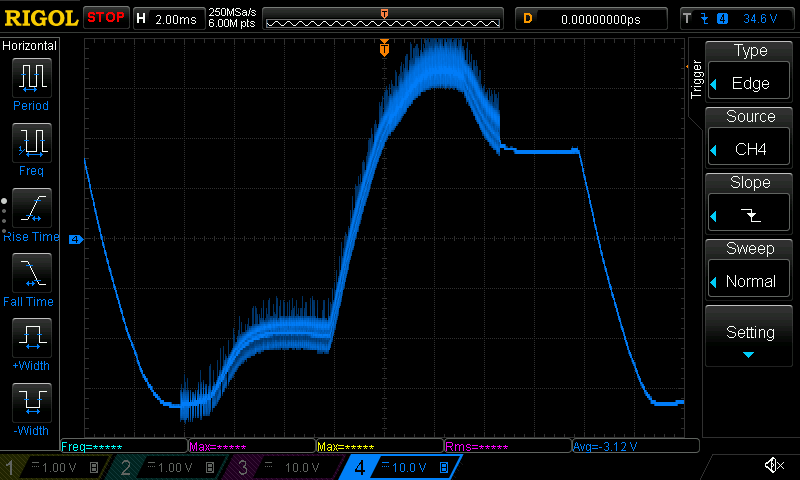
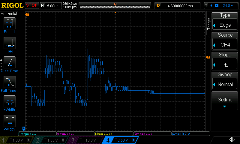
I use the UCC28911 as shown in the schematic, but it only works if the GND pin of the controller is connected to PE via a capacitor. The VS voltage at a successful start is shown in figure 2 and 3. A failed startup is shown in Figure 4 and 5.
It seems that the greater noise on the VS pin, when not connected to PE, triggers the OV protection.
Is there any way to fix this problem without requiring a PE connection for filtering?
Thanks in advance.
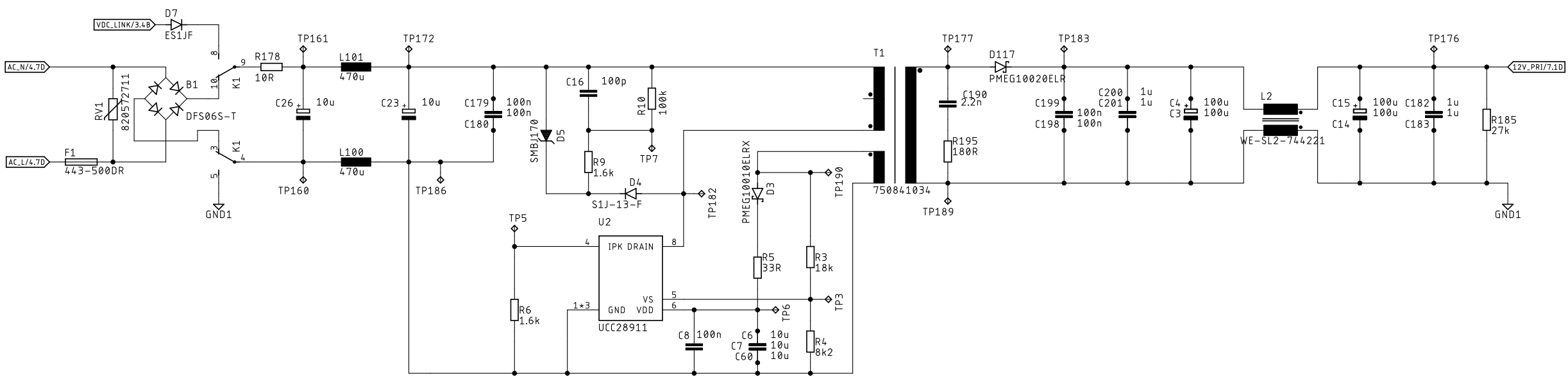 Figure 1
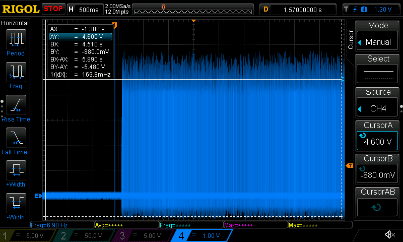
Figure 2: successful startup (PE connected to GND via a capacitor)
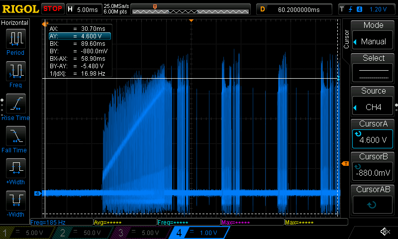
Figure 3: successful startup (zoom)
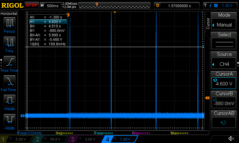
Figure 4: failed startup
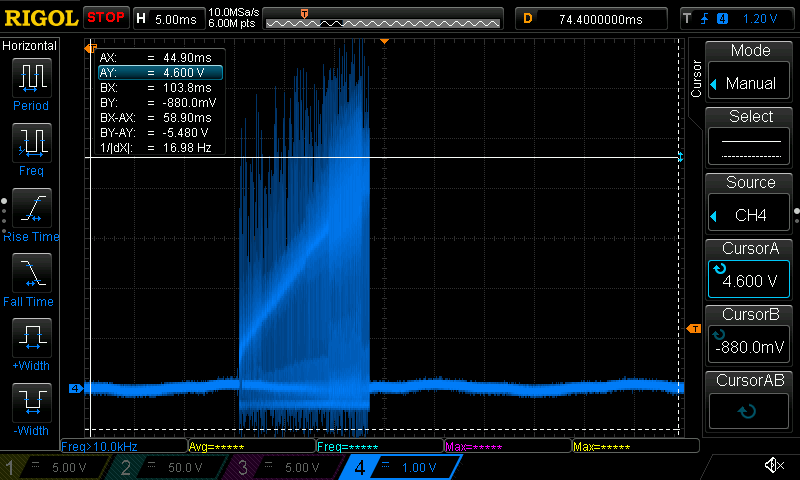
Figure 5: failed startup (zoom)