This thread has been locked.

If you have a related question, please click the "Ask a related question" button in the top right corner. The newly created question will be automatically linked to this question.

BQ25125: Load Switch in Bq25125

Part Number: BQ25125

Dear all,

A couple questions regarding the BQ25125 please.

1- What is the difference between the LDO and LS.  I understand the LDO is the regulated output, but I am not sure what it means when it is selected as load switch, please?

2- My understanding is when the BQ25125 is selected as a ship mode enable to be enable restore the power is hold the button connected to the MR low for a designated time.  Second way is to restore the power by 

     inserting power to the Vin.

3- If we connect the MR pin to a switch use for other purposes would it be, okay?

Thanks.

  • Hello,

    1- What is the difference between the LDO and LS.  I understand the LDO is the regulated output, but I am not sure what it means when it is selected as load switch, please?

    A load switch is effectively a simple way to enable or disable 

    2- My understanding is when the BQ25125 is selected as a ship mode enable to be enable restore the power is hold the button connected to the MR low for a designated time.  Second way is to restore the power by 

         inserting power to the Vin.

    This is correct.

    3- If we connect the MR pin to a switch use for other purposes would it be, okay?

    What purpose would you be using it for? The MR pin would retain its functionalities, though holding the MR pin to ground can increase quiescent current consumption for the duration that it is pulled low.

    Best Regards,

    Juan Ospina

  • Dear Juan,

    What I understand when the Load Switch selected then this pin acts something like the GPIO of a microcotroller, to enable and disable external component?

    So, over all we can have two LDO's based on BQ25125.  One if we select the LS/LDO as LDO and the second one SYS.  If so, can we change the SYS regulated output?

    Does BQ25125 has a monitoring Voltage.?  Is yes, is it like a Fuel Guage?

    Thanks,

    mmsya.

  • Hi mmsya,

    What I understand when the Load Switch selected then this pin acts something like the GPIO of a microcotroller, to enable and disable external component?

    It appears that my last response was incomplete. The load switch is a simple way to enable or disable a rail like with a switch. Essentially it allows the user to disconnect the source from the load digitally. In this case the source would be attached to VINLS and the load would be attached to LS/LDO.

    In LDO mode, the LS/LDO voltage is meant to regulated and stepped down from voltage at VINLS. In load switch mode, the voltage at LS/LDO is meant to be the same as the voltage at VINLS.

    So, over all we can have two LDO's based on BQ25125.  One if we select the LS/LDO as LDO and the second one SYS.  If so, can we change the SYS regulated output?

    The BQ25125 can allow two step-down regulators. The LS/LDO can work as an LDO but the SYS is a switching converter which will allow you to regulate SYS output, but it isn't a linear converter. Yes, you can change the SYS output based on the SYS_VOUT register. It can provide from 1.1V - 3.3V.

    Does BQ25125 has a monitoring Voltage.?  Is yes, is it like a Fuel Guage?

    The BQ25125 has a voltage based battery monitor that gives an approximate reading of the battery voltage in relation to VBATREG (e.g. 96% of BATREG). Although this provides battery voltage approximation, additional calculations would be necessary to approximate remaining charge and accuracy would be limited. This feature was meant to be used with a simple 5 bar indicator.

    Best Regards,

    Juan Ospina 

  • Dear Juan,

    I have some further questions please,

    1- 

    How about when SYS_SEL = 00 or 10 please?

    2- I am not sure how to interpret the following table please,

    Under what condition the OUT Voltage would be 800 mV step.  I do not see 800 mV step in Table 9-19?

    3- When SYS_SEL = 01 or 11, I see the table follows SYS VOUT range but this not the case for SYS_SEL = 00 and 10.

    Warm Regards,

    mmsya.

  • Dear Juan,

    In addition to above questions,

    1- What is 1600 mV, 800mV and so on mean please?

    2- In page 29 I think LSW stands for V Load Switch?

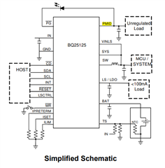
    3- From figure below I understand we can have 3 output Voltages 1- Unregulated Load, 2- MCU/SYSTEM (switching regulator) 3- LS/LDO.  The only difference that I see between LS/LDO is the Voltage range.  Both can be control through external pin and through I2C.

    Warm Regards,

    mmsya.

  • Hi mmsya,

    1- 

    How about when SYS_SEL = 00 or 10 please?

    For SYS_SEL = 00, then SYS = 1.1 + (a certain amount). The step size is not consistent for SYS_SEL = 00, from SYS_VOUT = 0000 to SYS_VOUT = 0001 the step size is 100mV, however from SYS_VOUT = 0000 to SYS_VOUT = 0001 the step size is 50 mV. It is best to consult table 19 for the typical voltages, for SYS_SEL = 00, when SYS_VOUT is greater than 0b0010 the step size is about 83.3 mV (1/12 of a volt).

    For SYS_SEL = 10 the SYS = 1.5 + SYS_VOUTCODE x 83.3 mV.

    2- I am not sure how to interpret the following table please,

    Under what condition the OUT Voltage would be 800 mV step.  I do not see 800 mV step in Table 9-19?

    To clarify, the SYS_VOUT_3 bit will have an 800 mV step when SYS_SEL is 01 or 11, not SYS_VOUT. SYS_VOUT will still have a 100mV step size. Since the step size for SYS_VOUT is 100mV, and SYS_VOUT_3 is Bit 3, the step size for this bit is (2^3) x 100 mV = 800 mV. So 800mV is the difference between SYS_VOUT = 0b0000 and SYS_VOUT = 0b1000.

    3- When SYS_SEL = 01 or 11, I see the table follows SYS VOUT range but this not the case for SYS_SEL = 00 and 10.

    Can you clarify, Which SYS VOUT range is not followed?

    1- What is 1600 mV, 800mV and so on mean please?

    This is similar to question 2 from before. In this table 1600mV and 800mV represent the step size of those individual bits. For LS_LDO_4 the step size is (2^4) x 100mV = 1600mV. So the difference between LS_LDO = 0b00000 and LS_LDO = 0b10000 is 1600 mV. The same is true for all the other values in the description column for the LS_LDO bits.

    2- In page 29 I think LSW stands for V Load Switch?

    That's right, the LSW indicates the device will behave as a Load switch rather than an LDO.

    3- From figure below I understand we can have 3 output Voltages 1- Unregulated Load, 2- MCU/SYSTEM (switching regulator) 3- LS/LDO.  The only difference that I see between LS/LDO is the Voltage range.  Both can be control through external pin and through I2C.

    This is correct, you can have an unregulated load from PMID, a load at SYS (switching regulator), and a load at LS/LDO.

    To clarify the difference between LS/LDO includes the voltage range but also the regulation that occurs. The LDO actively regulates the voltage at VLS/LDO to the programmed voltage and requires VINLS to be at least above the programmed voltage + dropout voltage. The LS requires that VINLS is regulated to the voltage that you would like at VLS/LDO.

    Please let me know if I can clarify any of the above answers.

    Best Regards,

    Juan Ospina

  • Dear Juan,

    Thank you for your time and replying to my questions.

    I will concentrate only on the output Voltages.

    1- If I understand you correctly you mention if we choose load switch, we have to feed a regulated Voltage to VINLS.  If this is correct, then why not use the LDO.  What would be an application of using the VLS please?

    2- Is MCU / System Voltage Regulated?

    3- Is unregulated Load at PMID Voltage the same as VBAT please?

    Warm Regards,

    mmsya.

  • Hi mmsya,

    1- If I understand you correctly you mention if we choose load switch, we have to feed a regulated Voltage to VINLS.  If this is correct, then why not use the LDO.  What would be an application of using the VLS please?

    This is correct, the voltage present at VINLS will be the same at VLS if operating as a load switch. This is in case the end application requires a voltage higher than 3.3V or lower than 0.8V. The load switch is ultimately there to provide the option to connect or disconnect a load from a power rail. Say, for example, you have a buck-boost 5V rail and you have some loads that should always be connected to it and some peripheral IC that you would sometimes want connected and sometimes disconnected. The load switch allows you to disconnect a load at VLS from a supply at VINLS. If it is more useful to have a regulated voltage between 0.8V and 3.3V than it may be more useful to keep the LSLDO in LDO mode.

    2- Is MCU / System Voltage Regulated?

    Yes, it is regulated to the voltage configured in SYS_VOUT.

    3- Is unregulated Load at PMID Voltage the same as VBAT please?

    PMID voltage will either be driven by VIN or VBAT. If in VIN mode, PMID will be equal to about VIN - 125mV. If in VIN is not present, PMID will be equal to about VBAT - 120mV. These voltages are equivalent to the voltage drop across the Q1/Q2 FET for VIN or the Q7 BATFET for VBAT. 

    Best Regards,

    Juan Ospina

  • Dear Juan,

    Thank you for all your time and effort you put to answer my questions.

    I have one further question please.  

    You mentioned in part one on the most recent post, "the voltage present at VINLS will be the same at VLS if operating as a load switch."  If this the case, then how would you explain LS/LDO = 0.8 V + LS_LDOCODE x 100 mV  (equation listed in Table 9-20) please?

    Warm Regards,

    mmsya.

  • Hi mmsya,

    To clarify, The voltage present at VINLS will be the same at VLS if you are in load switch (LS) mode. Table 9-20 is only relevant while in LDO mode. To select between the two modes you have to selected the LS/LDO voltage. If you set it to 3.3V or below (LS/LDO = 0b11001 or less) then the LSLDO will be in LDO mode and will be regulate VLSLDO to the configured voltage. If you set it to above 3.3V (LS/LDO = 0b11010 or higher) then the LSLDO will be in LS mode, or 'pass-through mode' and the voltage at VLSLDO will be equal to the voltage at VINLS - dropout voltage.

    I hope that clarifies things.

    Best Regards,

    Juan Ospina

  • Dear Juan,

    I do not see in the datasheet it specifies that the Table 9-20 is only relevant while in LDO mode.  I may have missed it.  So, here is my understanding that if I select the LS/LDO in LS mode whatever the SYS_OUT Voltage is VLS is as well. We can set the SYS_OUT Voltage to a value and then VLINS connected to the SYS_OUT therefore VLS is the same as SYS_OUT.  In this case we only have one regulated Voltage.  If we choose the LDO mode we select any output as we wish according to LS/LDO = 0.8 V + LS_LDOCODE x 100 mV formula.  Would not be more clear if they had printed LDO = 0.8 V + LS_LDOCODE x 100 mV formula instead of LS/LDO.

    Again thank you for your valuable tim.

    Warm Regards,

    Ali.

  • Hi Ali,

    If I understand correctly, in this scenario you would connect your VINLS to your SYS output. In this case, your VLS/LDO voltage will be the same as SYS. If you change the SYS voltage then VLS/LDO will also change to match that voltage.

    If you choose LDO mode output will be according to the formula  LS/LDO = 0.8 V + LS_LDOCODE x 100 mV. Please keep in mind that if you are using the LS/LDO in LDO mode, VINLS has to be above the programmed voltage in order for VLS/LDO to output the programmed voltage.

    Thank you for the feedback, we will consider this when writing the datasheet. At the bottom of the table it should indicate:

    "If a value greater than 3.3 V is written, the setting goes to pass-through mode where LS/LDO = VINLS - VDROPOUT."

    Best Regards,

    Juan Ospina