This thread has been locked.

If you have a related question, please click the "Ask a related question" button in the top right corner. The newly created question will be automatically linked to this question.

TPS7A85: Serial vs Parallel Design for high reliability

Part Number: TPS7A85
Other Parts Discussed in Thread: , TPS7A83A, TIDA-01232

Hi all, I need some advice.
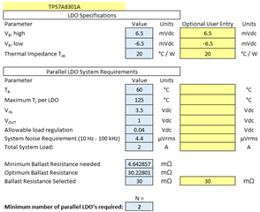
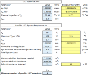
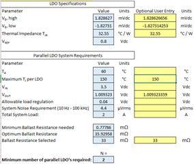
I have to use the TPS7A85 component to meet the following parameters:
Input Voltage: 3.5V
Output Voltage: 1V
Output Current: 2A
Allowable Ripple : 1mV
Voltage Tolerance: 3%
Operating Temperature: up to 60 Deg.C
EN and Power Good Pin used
I can't use a DC-DC to step down the voltage before the LDOs.

To maximize the reliability of the circuit that will have to operate continuously for a long time (years), I was thinking of using two TPS7A85.
A serial design would be very easy to implement, but could be more prone to failures.
A parallel design instead would be intrinsically safer (it would work even with a broken component), but it is more complicated to implement.

What solution do you recommend?
Thanks in advance.
Regards.

  • Hi Antonio,

    We would recommend the TPS7A85A over the TPS7A85.

    What is the maximum AC ripple voltage on Vin?

    We have brand new white papers and an easy to use calculator that shows how to parallel LDOs using ballast resistors (see below).  The calculator will help you answer the question on how many LDOs you need given a set of design requirements.  We are still adding LDOs to the calculator, and I can look into what it would take to add the TPS7A85 later today.  The bottom line is paralleling with ballast resistors is no longer difficult, even for a worst case analysis, and even for more than 2 parallel LDOs. 

    It looks to me like the benefit of serial connection is better PSRR, and the benefit of parallel is intrinsically safer.  Unless the ripple on the input is very high, you would be better off with a parallel connection.

    Thanks,

    Stephen

    New, comprehensive design resources are available for paralleling LDOs using ballast resistors. 

    A Scaleable, High-Current, Low-Noise Parallel LDO Reference Design [NEW]
    Comprehensive Analysis and Universal Equations for Parallel LDO's Using Ballast Resistors [NEW]
    Parallel LDO Architecture Design Using Ballast Resistors
    [NEW]


    Simple calculator for complex parallel LDOs
    PARALLEL-LDO-CALC [NEW]

  • Hi Antonio,

    I hope to have the next revision of the calculator updated in 1-2 weeks, and I've added the TPS7A85A and TPS7A83A.  You will want to use the TPS7A83A because it comes in the RGW package with much better thermal resistance (33.4 C/W for the RGW package vs 43.4 C/W for the RGR package).  Note that these thermal resistance values are based on the 2s2p JEDEC spec.  Most customers can achieve significantly better thermal resistance than the JEDEC spec by placing more ground copper and thermal vias in their design - our EVM's regularly achieve up to 40%-50% improvement. The customer will want to achieve a 20 C/W thermal resistance in their design (parallel or series), which may be difficult with the RGW package but should be doable with the RGR package. 

    Keep in mind that it is the junction temperature of the device which sets the long term reliability (and ability to operate for years).  Our LDOs are characterized at 55C.  You can find the reliability of the TPS7A83A (or any TI LDO) by going to its product folder, or by going here:

    https://www.ti.com/quality-reliability-packaging-download/report?opn=TPS7A8300ARGWR

    Using the links on the left side, you can find the temperature change FIT and estimate the MTBF at elevated temperatures.  For this device, even at 125C there is still a lot of life in the component.

    The customer will want to use the smallest resistor values possible to set Vout (Vref is 0.5V so to achieve 1V output, the high side and low side setpoint resistors are the same).  They will want to use 0.5% tolerance to help with meeting their 3% tolerance requirement. The new error voltage is +/- 1.2mV plus the setpoint resistor tolerance.  For example, 7.8k setpoint resistors gets us to +/- 6.5 mV (it will be basically the same answer for 1k setpoint resistors, etc).  The results of the worse case calculator are shown below.

    If they have a known minimum load current, which is not 0A, we can try using that to our advantage.  Parallel LDOs using ballast resistors have a DC drop due to the small ballast resistance, and we can offset some of that drop by raising Vout if there is a nonzero minimum load current.  Let me know if you wish to pursue this and I can run monte carlo simulations to find the best resistor combination.

    Thanks,

    Stephen

  • Hi Stephen,
    Thanks for your reply and the documentation you attached.
    I'm reading it and I'm definitely feeling more confident about a parallel design.
    The reliability and the estimated MTBF are also reassuring but, unfortunately, I am forced to use only the TPS7A85 for "corporate" reasons.

    At this point, following a design similar to TIDA-01232 (but with discrete ballast resistors instead of tracks) seems a good idea, what do you think? But i haven't done all the calculations yet and I suspect that, for the parameters I need, just two TPS7A85s in parallel might not be enough.

    As soon as updated, i will definitely try the excel calculator. I was just wondering if compensation for the voltage drop across the ballast resistor is included in the calculations, to keep output voltage btw the parameters .

    Thanks again for your help!

    Antonio


    p.s.
    in this component the difference VIN-VOUT= 2.5V is only a problem of dissipated power, and there are no other limitations, right?

  • Hi Antonio,

    Hopefully this is clear but I know this can be a lot to take in.  Let me know if you would like a video chat to go over these options.

    You will want to use the math from the links I sent to you, don't use the math in the TIDA-01232.  That reference design uses older techniques on the ballast resistor problem which do not scale well beyond 2 LDOs.  And yes, you probably want a discrete resistor instead of a PCB trace.

    Yes, the voltage drop across the ballast resistor is included in the math.  The ballast resistor is in series with the PCB trace resistance (forward path and return path) so technically, the ballast resistor + PCB trace loss is all included in the calculator automatically.  And you are correct - there are no other limitations except the power dissipation due to Vin-Vout = 2.5V.  (I am assuming the ripple voltage on Vout will be easy to achieve but you will want to review the Vin AC ripple with the PSRR of the LDO datasheet to obtain your expected Vout ripple.  It should be well under 1mV though, let me know if it is not).

    The screenshot of the MS Excel calculator shows your use case with the parallel TPS7A85A.  If I change that to TPS7A85 (no revision A) the only difference is the thermal resistance which will unfortunately go up.  Everything else is the same in the calculator.  Your power dissipation is the main limitation here, and it does not matter if you parallel them or place them in series.  I would find out if there is a metal chassis or screw hole nearby that can act as a heat sink.

    If we increase the allowable temperature to 150C, we can keep the LDO's down to 2 but obviously this will lose additional life from the LDOs.  3 parallel LDOs might be easier with the TPS7A85, is that possible in the design?  Using the TPS7A85 in a thermally saturated design, lets say you can get a 40% improvement in thermal resistance (which is not as good as we see in our EVMs so this should be doable).  3 parallel LDOs will stay under 125C but in the event that one fails, 2 parallel LDOs will still meet the voltage and current requirements while staying under 150C.  So you still get your reliability if one LDO breaks after years of use.

    Another option is to place a series resistor in front of the LDOs to dissipate some of the heat.  This chokes off the line voltage so we would need plenty of decoupling on Vin to maintain performance during a load transient, or ensure a monotonic startup during turn on. You probably don't save any board space but it is possible you save some cost at the expense of some performance.

    Thanks,

    Stephen

  • Hi Stephen, sorry for the delay in responding but it's been a hard day at work.

    First of all I would like to thank you for your extreme availability, really helpfull. 

    I don't like the idea of the resistor in series in front of the LDO, but the possibility of adding a heatsink, or dissipate through the metal casing of the device, is interesting and feasible.In this regard, do you have any particular suggestions about the design of the thermal pad of the VQFN packages? In particular how the number (5 or 9) and size (0.2 to 0.3) of vias affects performance.

    I'm planning to produce a small prototype in order to test the design with 3 TPS7A85 LDOs in parallel. As you advised, to size the ballast resistors (with discrete components) I'm going to use the docs you attached (so not TIDA01232). In the next few days I'd like to ask for your help to validate these calculations.
    Thanks again,

    Antonio

    p.s. After further verification the power supply rejection should be well within the specifications of a single LDO (and therefore also of 3 in parallel). It will be tested on the prototype anyway.

  • Hey Antonio,

    I would be happy to review your draft schematic when you are ready.  I'll respond in a new message on PSRR testing.

    I would recommend shifting Vout to 1.01V so you can allocate more tolerance to the voltage droop associated with PCB trace resistance and the ballast resistors.  You should still meet the +/- 3% DC spec with this slight increase in Vout.  I took another look at the TPS7A85 datasheet and I always forget that Vref for that is 0.8V (as opposed to Vref for TPS7A8301A, which is 0.5V).  Here is an updated (unreleased) calculator results.  I'm experimenting with a method to include effects of feedback resistor tolerances so customers (and I) don't have to mess with that.  What you see here should be a worse case approach to feedback resistor tolerance and includes the +/- 1.2mV offset voltage being gained up slightly by the feedback resistor gain.  I would go with 0.5% tolerance resistors with values of 3.48k and 13.3k (this gets you almost 1.01V typical from 0.8V reference voltage).

    In the event you see close to 150C operation (1 LDO fails) then the ballast resistors may also see that temperature.  But your power dissipation across the ballast resistors is small.  Something like an 0603 rated at 0.2W will probably work as long as it is rated for 170C (review the derating curve).  An 0805 resistor might be cheaper and easier to find - please look around and see what's best for you.  It looks like 33 m-ohms is the ballast resistor to select assuming 25% reduction in thermal resistance from the JEDEC spec (should be doable).  Even if you have 4 m-ohms of PCB impedance in series with this, it won't change the results.  3 LDOs will keep the temp below 125C and if one fails, 2 LDOs will stay below 150C and continue delivering the load.

    Add as many via's into the thermal pad that you can fit and also manufacture.  Heat radiates out of the surface of the PCB, so focus on large, thick ground planes on top and on the bottom of the PCB where the LDO will be located.  PCB manufacturers worry about solder flowing through the vias so they may automatically plug the via with a conductive fill.  Conductive fills are thought to be less thermally conductive than pure copper.  If you can tent the via on the back side of the PCB this may stop the solder from flowing out of the PCB, while still providing a better thermal path than conductive fill.  I would ask your fab house what the best approach is here.  I add thermal vias around the LDO wherever I can as long as they are not interrupting the flow of current.  In our EVMs there is almost always one side of the LDO which can be used to add thermal vias (usually above or below the LDO).  Exposing the PCB copper around the LDO (if possible) by removing the solder mask, and adding a metal chassis heat sink would be great.  You probably need thermal interface material (TIM) if you do this.  Adding a metal heat sink to the back of the PCB under the LDO is also good, but the volume of metal you add will want to look meaningful when compared against the PCB itself.  (I.E. adding a tiny heat sink to a large, 2 oz multilayer PCB is probably not going to achieve anything you can measure.  But attaching a 2 pound aluminum chassis to a small PCB will have a significant effect).

    There is some scientific discussion online which suggest that the color of solder mask can make a difference.  The idea is that heat radiates more from a black solder mask than something like white.  So in theory, black solder mask is better than green or white.  We don't have any app notes on this but I wanted to let you know in case you think this would be something that could help.

    Thanks,

    Stephen

  • Hi Antonio,

    To measure the PSRR you will want to reduce the input cap as much as possible.  The TPS7A85 is designed and characterized with 5uF effective capacitance or more at the input.  You might be able to get this lower, say 2.2uF, for the PSRR testing.  It can be difficult to drive microfarads of capacitance at high frequency (usually above 100 kHz but definitely 1MHz or higher.  Basically where the cap resonates and you are driving the ESR of the cap with a sine wave).  I've noticed that I need more signal at low frequencies until the PSRR peak occurs and the PSRR starts to decrease.  Then I back off on the PSRR injection level quickly, well within a decade. 

    Hopefully this will help get you to a clean measurement.

    Thanks,

    Stephen