This thread has been locked.

If you have a related question, please click the "Ask a related question" button in the top right corner. The newly created question will be automatically linked to this question.

TPS55289: Schematic check, especially loop compensation circuit

Part Number: TPS55289
Other Parts Discussed in Thread: , LM5177, LM5176

Hello Engineers,

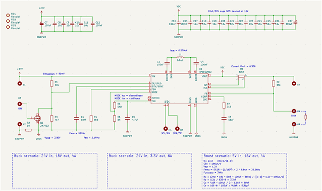
I'm designing a dc/dc converter around the TPS55289 (and TPS552892) and have calculated the loop compensation components for a 5->18V 4A boost converter.

This design will also be used as a buck converter (24->3.3V 5A) and I would like to know how it behaves in this situation. Do I need to change the loop compensation circuit for buck operation? I'd like to run the converter at 2100KHz to reduce the output ripple as much as possible, does the junction temperature stay below maximum at 2.1MHz?

The 6.8uH, 4.1mR, 22A Wurth 7443556680 will be used as the inductor.

TPS55289 schematic

  • Hi Roy,

    TPS55289(and TPS552892) is not suitable for this application. For buck mode, it could be used in 24->3.3V 5A condition. In boost mode 5->18V 4A, the average inductor current needs to be 18V*4A/5V/0.9=16A. It's much higher than TPS55289 average inductor current limit 8A typ.

    I would suggest you consider using TI buck-boost controller LM5176, LM5177.

  • Then I'll just have to temper my expectations in boost mode and specify the output current limit to 2A. I'll also pick a smaller inductor as the load is significant less then what the Wurth inductor can handle. 

     Thank you for your feedback Zack!

  • Hi Roy,

    18V/2A is still too high load for 5V Vin condition. 

    Below are comments on the schematic:

    1. For this application, suggest set the fsw at 400kHz to avoid too much power loss on the IC. It's still ok to use 6.8uH inductor Wurth 7443556680 . Change the Fsw pin resistor to 49.9kohm.

    2. For TPS55289 (I2C version), MODE pin select the I2C slave address. You need to configure the I2C register first. For TPS552892 (non I2C version), the MODE pin select the working mode between FPWM mode and PFM mode.

    3. SCL, SDA, (CC/PG) need pull-up resistor to 5V or 3.3V if you use these two pins.

    4. If you use TPS552892 (non I2C version), the feedback bottom resistor need to be soldered. The two feedback resistors need to be placed very close to FB pin to avoid noise coupled to feedback and compensation loop.

    5. Compensation: R7 20kohm, C5 10nF, add a 100pF cap across COMP pin and AGND pin.

  • Hello Zack,

    Thanks again for checking my schematic. I plan on putting this schematic on a 1/8th brick based PCB. Then use external components to decide on the specific function. So the pull-up and bottom feedback resistor will be placed off-board close by. I wish to design a single PCB with two different BOMs and schematics.

    I'll change the frequency to 400KHz, I was hoping that I could use >2Mhz to limit the output ripple.

    Thank you for noticing 2, I'll change the schematic for the TPS55289 version so that it will just pull-down with a 10R link.