This thread has been locked.

If you have a related question, please click the "Ask a related question" button in the top right corner. The newly created question will be automatically linked to this question.

TPS62823: SW pin over-current after UVLO

Part Number: TPS62823


Hi.

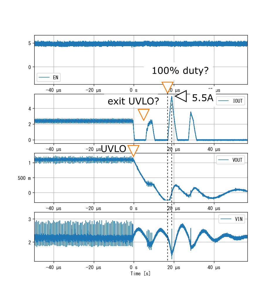
I'm observing SW pin over-current when a device goes into UVLO while VIN is ringing badly. Is this behavior normal for this part?

Measured peak current at SW pin is about 5.5A, which is far beyond the operating conditions and above High-Side FET Current Limit (max). I could reduce ringing at VIN by adding more capacitors, but I would like to know why this part is behaving like this.

Best regards.

probe points

  • Hi,

    The current limit functionality doesn't work when the VIN is below UVLO. It seems to me there is some high inductive transient load as the output is seen to go even negative.

    Can you repeat this with all loads on the output disconnected? You could also try disabling the converter via the EN pin before ramping down VIN.

    Best regards,

    Varun

  • I forgot to mention that my test setup used an electronic load to draw constant current of 2.4A. If I set electronic load to draw 2.0A, IC does not behave like 100% duty mode as shown in previous post. If I disable the converter via the EN pin before shutdown, UVLO will not be triggered and stops safely.

    (↓with 2.4A load. EN-OFF before shutdown.)

    shutdown by EN off

    (↓with 2A load. Probed SW pin voltage instead of current because I do not have current probe set up right now.)

    (↓ with no load)

  • Hi,

    Thanks for the scope shots. The problem you saw seems to be caused by inductance of the long cable wires and the electronic load. Can you please run the tests with a resistive load soldered on the board itself? I don't think you should see the problem

    Best regards,

    Varun

  • Hi,

    I think this conversation is derailing a bit. My original intention of the question is about "how this part is conducting large amount of current after UVLO" and not about "how to reduce ringing". The latter part is already solved by adding caps or shutting down by Enable pin. The former part is concerning because either one of my assumptions below is not satisfied.

    1. During normal operation (at VIN > UVLO), OCP should trigger at most 5A.

    2. During VIN < UVLO, both high-side and low-side FETs are turned off. Thus only body-diode can allow a current to flow.

    Can you clarify what I'm misunderstanding about the behavior of the device?

    Best regards,

  • Hi ,

    Are you referring to the inductor current (5.5A) in the area highlighted by the red circle? From what I see in the graph, the VIN is < 2V and UVLO limits in this area. Both the FETs are shutdown and the device is turned off. It is not is 100% duty cycle as marked in the graph. The current limit functionality doesn't work when VIN is below UVLO.

    The flow of inductor current is through the body diode of the low side FET. 

    Let me know if there is still some confusion.

    Best regards,

    Varun

  • I'm sorry. I accidentally clicked "This resolved my issue" button. Can I reopen this post?

    I checked SW voltage at 2.4A load. What I'm still confused about is that, just before the peak current, SW voltage is high (marked in orange circle). Is this caused by body diode?

  • Hi,

    No problem, the thread gets automatically re-opened when you comment on it. 

    Since VIN is oscillating and at the border of UVLO operation, you see some areas where the device tries to restart. The area highlighted in orange indicates the high side FET is on. It is not technically in 100% duty as VOUT is negative. The VIN here goes down to only about 1.5V unlike the first picture where it went down to 1V. Would be good if you can add inductor current as well to the last scope shot.

    Best regards,

    Varun

  • Hi.

    Attached two more scope shots. Green trace (CH2) is inductor current.

  • Hi,

    Thanks for the scope shots. In one of them, the inductor current goes pretty high. For the current limit, the ac peaks can also exceed the static limits in the spec table. This is because of a 60ns internal propagation delay. Please see section " 8.4.4 Current Limit and Short Circuit Protection" in the datasheet.

    The chances of such a situation happening in a practical application could be low as you need an overcurrent condition with a long wire to make VOUT negative.  

    Best regards,

    Varun

  • Hi,

    Thanks for the explanation. So, deciding from the scope shot taken before, the OCP is triggered about 300-ns after reaching 5A. I think this is much longer than typical value of 60-ns. Is this expected OCP behavior? Also, why high-side FET is on for nearly 1.9µs in the first place?

    The chances of such a situation happening in a practical application could be low as you need an overcurrent condition with a long wire to make VOUT negative.  

    Do you mean this is the expected behavior of the device when VOUT goes below 0V?

    Best regards.

  • Hi,

    The 300ns is longer than expected. The VIN could be on for 1.9us because the device starts up in PFM and there probably is a small delay before the UVLO circuit kicks in.

    We usually don't test it in this case where VOUT is pulled negative and VIN also oscillates close to the UVLO levels. The negative VOUT could be having an influence on the internal current limit clamps. Do you see this problem on your board if VOUT doesn't go negative?

    Best regards,

    Varun

  • Hi,

    I understand that this condition is unusual, but we need to clear this concern up to use TPS62823 for next project.

    Do you see this problem on your board if VOUT doesn't go negative?

    Simply driving VOUT pin negative did not cause this problem. It also didn't happen at slightly different conditions like 2A-load as shown in previous post.

    Best regards,

  • Hi,

    I discussed about this with the designer and he mentioned this is expected operation as the UVLO circuit has a certain delay (~2us). Since the VOUT is 0V, the converter will turn on the high side FET for a longer on time. The max current limit of 5A, in the datasheet is valid only for VIN=2.4V to 5.5V.

    Best regards,

    Varun

  • Hi,

    Thank you for the reply. These information are very helpful.

    The VIN could be on for 1.9us because the device starts up in PFM
    Since the VOUT is 0V, the converter will turn on the high side FET for a longer on time.

    I'm still not sure about this. The device should run at constant on-time control unless it is running at 100% duty mode right?

    Also, If the datasheet is only valid for VIN=2.4V to 5.5V, does that mean nothing is guaranteed when VIN is between UVLO and 2.4V, or at the duration of UVLO delay?.

    Best regards,

  • Hi,

    The DCS control topology used in this device, is able to extend on-time if the output voltage is low. The following app note describes this https://www.ti.com/lit/an/slyt531/slyt531.pdf. Figure 3 in the app note shows a similar extension of the on time during a load transient.

    We usually only provide a current limit spec for the recommended VIN operating range. When the device is for example at the UVLO delay, the internal propagation delay could be longer than the typical 60ns, because of the low VIN during this time.

    Best regards,

    Varun