This thread has been locked.

If you have a related question, please click the "Ask a related question" button in the top right corner. The newly created question will be automatically linked to this question.

CSD97396Q4M: power cycling the application kills MOSFET

Part Number: CSD97396Q4M

Hello,

I'm working on a cooler design that uses two buck converter stages comprising the CSD97396Q4M.

The load (peltier element) is connected to the output of the converter stages to essentially build a H-bridge.

Below find the schematic of one half of the H-bridge.
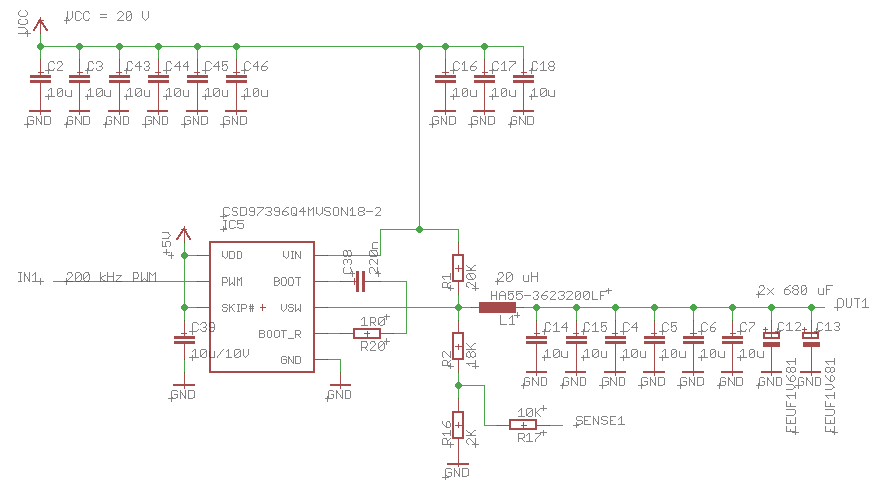
The H-bridge is controlled by a PWM signal with a frequency of 200 kHz. The other half of the H-bridge is identical but sees the inverse PWM signal.

At 50% duty cycle, both outputs of the two H-bridges have about VIN/2, so the load sees no voltage difference. Changing the duty cycle from 50% will put a voltage across the load. That's the theory.

However, this design does not work reliably. Switching the cooler unit off and on will damage the part permanently. That is, one of the  FETs of the power stage fails with a short circuit (to VIN or to GND or both).

Why is this?

I'm observing strong ringing on the switching node. To reduce ringing, I increased the boot resistor to 4,7 Ohm but that did not help. Adding a Schottky diode between switching node and VIN  (i.e., parallel to body diode) did not help, either.

This is the signal on one of the two switching nodes.

Scope Shot

Although the switching node rings that does not seem to kill the part. It seems to withstand this stress.

However, powering off and on of the cooler a couple of times does kill it the part.

Please advise.

Thanks.
Dan

  • Hi Dan,

    Can you please share the complete schematic to clear some of my doubts. Also, I have following questions. 

    1. SKIP# is High. What is status of Low side switch (ON or OFF) when the device is turned OFF?

    2. The device which turned OFF, and then turned ON is showing failure. Correct??

    3. What is VOUT of the device, just before it is turned ON.

    4. Can you provide inductor current waveform at the failure instant. 

    Regards

    Vasav 

  • Hi ,

    Thank you for your prompt response.

    You are asking for a complete schematic, however, what you see above is basically the whole schematic regarding power stage. What is missing is the second half of the H-bridge, but it's a copy of the first half, except that it's controlled by the inverted PWM signal. Further, the linear regulator for 5V is not shown and the circuit for the PWM signals is not shown.

    That's the basic configuration of the circuit:

    Each green box represents a CSD97396Q4M.

    When I test the design, I'm using a 50% duty cycle PWM with 200 kHz.

    What other information about the circuit do you need?

    Now I'll try to answer your questions as best as I can:

    Re Q1:

    Which low side switch do you mean? I assume that the FETs inside the CSD97396Q4M are toggled according to the PWM frequency. I can't tell in which state they are when the cooler is switched off. Further, there's no shutdown procedure. The running system is just switched off by the flick of the power switch.

    Re Q2:

    I don't know, see Q1.

    Re Q3:

    I assume that with Vout you are referring to the voltage at the inputs of the load. In my tests, I'm running the PWM at 50 % duty cycle. That is, the load sees 10 V at each input and there's no voltage across the load.

    Re Q4:

    Sorry, no. 

    While I read your questions, I think we have a misunderstanding regarding the term "device" and which "device" is switched on and off. I guess that you mean the CSD97396Q4M part while I'm talking about the cooler unit. For avoidance of a doubt, during my tests, the CSD97396Q4M part failed after the cooler system had been switched off and on again. It does not fail during "runtime".

    Thanks for you support.

    Best regards,
    Dan

  • Hi Dan,

    Sorry for the confusion. Let me clarify my statements.

     All my questions are related to the device (CSD97396Q4M) which is failing.

    From your answers I get following impression

    1. Output of the failing buck converter is zero. This implies that low side FET was ON

    2. You are not using soft start. 

    3. Duty cycle is fixed to 50%, with VIN=20V

    Possible cause of failure.

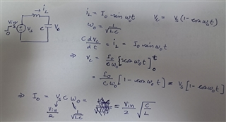
    1. This circuit will have high LC resonance. Amplitude of the average inductor current is VIN/2 * sqrt(C/L) ~ 86A.

    2. I asked you inductor current waveform just to confirm this fact. 

    Possible solution:

    1. Use soft start. (preferred)

    2. reduce capacitance and/or increase inductance. => This approach may cause problems related to meeting transient performance. 

    Regards

    Vasav 

  • Hi Vasav,

    Thank you for providing assistance.

    I agree with your impression #2 and #3. However, what gave you the impression #1 that "Output of the failing buck converter is zero"? As I mentioned, the failure mode I observed is "short circuit" but it could be from switching node to VIN or from switching node to GND. 

    Further, could you please explain why this circuit has a "high LC resonance"? I don't know how you derived that equation that us used to calculate the inductor current of 86 A. I have no idea what would generate that high an inductor current. Most of all as there is no relevant voltage across the load at PWM duty cycle of 50%. Please elaborate your findings. 

    Regarding "inductor current waveform", please advise me how to measure the inductor current. I have a oscilloscope and can measure voltages. The circuit is on a PCB and there's no way that I could add an shunt resistor to it without redesign.

  • Hi Daniel,

    Thanks for reporting disagreement with impression #1. 

    From your previous reply, I can say the output of the failing buck converter (CSD97396Q4M) is 10V, just before turning it ON. In this situation my calculations for inductor current would not hold. 

    I have following concerns.

    1. Is this topology already verified? 

    2. Do you experience same blowup issue on interchanging the two sides of the Load. --> If device A is turned OFF and ON. Repeat with device B turning OFF and ON

    3. With 20 V DC, the switch node is reaching to >35V. Whereas VDS in CSD97396Q4M is designed for 30V only. Are you following TI recommendation for layout and schematic designs?

    4. Since MOSFET generally fail by high current and Voltage, I need inductor current waveform also to reach to a conclusion.

    Regards

    Vasav 

  • Dear Vasav,

    You write "the output of the failing buck converter (CSD97396Q4M) is 10V, just before turning it ON". In a synchronous buck converter, there are at least two switches. To what element do you refer when you write "before turning it on"? Further, the power stage includes two MOSFETS which are alternatingly turned on and off according to the to the PWM input signal. Otherwise there would be not output signal of 10 V.  Thus I think your statement does not properly reflect the working of the buck circuit.

    Basically, I just can't make much sense of your use of the words "on" and "off" in the context that you use it ("If device A is turned OFF and ON. Repeat with device B turning OFF and ON"). The design comprises two synchronous buck converters, that is two CSD97396Q4M. In total, there are four switches (see my drawing above) and they all switch on and off perpetually following the 200 kHz PWM input signal.

    Regarding "layout", I'm under the impression that the layout adheres to TI's commendations.

    Regarding "inductor current waveform", please propose a pragmatic way to measure this waveform.

    Thanks
    Daniel

  • Hi Daniel,

    Sorry for the delayed reply. Before answering other questions, I need to clarify following.

    1. Device (CSD97396Q4M) off means --> PWM is tri stated 

    2. FET OFF --> FET is not conducting (TON/TOFF duration of a switching period.)

    Based on your comment in first paragraph it seems that PWM is not tri stated, and both Buck converters are active all time. Correct??

    With this understanding I have following concerns on the design.

    1. As mentioned earlier, because of absence of Soft start --> FET current can go to 86 Amp. This assumes that both CSD97396Q4M are sharing equal current. Otherwise current stress will be even higher.

    2. Switch voltage spikes are quite high (35V). Allowable limit is 30V. TI layout recommendation needs to be followed

    3.  Measure inductor current. --> Can you put a wire loop to measure the current. 

    Regards

    Vasav 

  • Dear Vasav,

    For clarification, PWM is "tri-stated" only system startup: a tri-state buffer LVC2G126 feeds the PWM signal to the device CSD97396Q4M. When the system is switched on, the buffer output is tristated (floating), i.e., the device CSD97396Q4M is disabled. Then a PWM with 50% is generated and the buffer is enabled, i.e., the device CSD97396Q4M is enabled. From this point on, both Buck converters are active all time.

    Regarding your concerns:

    1. Could you please elaborate on your finding of "Amplitude of the average inductor current is VIN/2 * sqrt(C/L) ~ 86A." How did you derive that equation? Is there an app note with more details?

    2. The switch voltage spikes might look like 35V on the scope shot above but if I choose a shorter time resolution, they do not exceed 30V. Further, as I mentioned before, failure does not occur during runtime of the system but rather when powering up/down.

    3. I measured the current through the load with a clamp on meter. However, currently I have no fully working PCB at hand that I can use for my measurements. So I measured a PCB where one buck converter has failed  and pulls the respective load connection to GND. The other side of the load is connected to the working buck converter. PWM is at 50% duty cycle and that buck converter outputs VCC/2. That results in a current of 11 A through the load.

  • Hi

    It is india holiday and Vasav will reply you tomorrow.

    Regards

    Yihe

  • Hi ,

    No worries, mate. I'm not in a rush.
    Thanks for letting me know.

    BR,
    Daniel

  • Hi Daniel,

    Answers to your concerns is below. 

    1. Concern1 - 

         The derivation is given in above image. An obvious question could be why did I choose Vs = VIN/2. The reason is that the duty cycle is 50%. 

    This calculation has some assumptions --> (1) Both buck converters are identical. (2) impact of switching is neglected. (3) PWM freq. is much higher than the LC resonance freq. (4) All non-idealities (eg. FET/trace resistances, dead time) are neglected. (5) inductor is in linear region (not saturating). 

    2. Concern 2 - This seems that high spikes are not the concern. But, your comment "failure does not occur during runtime of the system but rather when powering up/down" gives an impression that high current is killing the MOSFET. As mentioned in first comment, this current would be ~86A. Of course to validate this fact, inductor current measurement is required. 

    3. Concern 3- Inductor and load currents are independent during transients. Therefore information of inductor current cannot be obtained from the load current. 

    Possible solutions are

    1. Reduce output capacitors. (~ 1/10 of present value) --> This will reduce the peak current of the inductor. 

    2. Use soft-start.